SK Hynix Adds HBM2 to Catalog: 4 GB Stacks Set to Be Available in Q3
by Anton Shilov on August 1, 2016 10:00 AM EST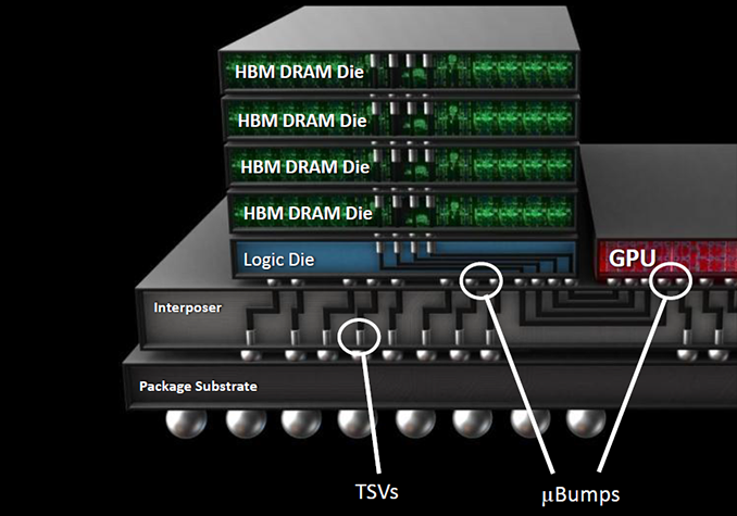
SK Hynix has quietly added its HBM Gen 2 memory stacks to its public product catalog earlier this month, which means that the start of mass production should be imminent. The company will first offer two types of new memory modules with the same capacity, but different transfer-rates, targeting graphics cards, HPC accelerators and other applications. Over time, the HBM2 family will get broader.
SK Hynix intends to initially offer its clients 4 GB HBM2 4Hi stack KGSDs (known good stack dies) based on 8 Gb DRAM devices. The memory devices will feature a 1024-bit bus as well as 1.6 GT/s (H5VR32ESM4H-12C) and 2.0 GT/s (H5VR32ESM4H-20C) data-rates, thus offering 204 GB/s and 256 GB/s peak bandwidth per stack. Earlier this year a representative for SK Hynix revealed plans (in an interview with Golem.de) to start volume production of 4 GB HBM2 KGSDs in Q3 and the addition of the devices into product catalog confirms this information. Keep in mind that memory companies usually make announcements about the start of mass production when they are ready to deliver the first batch of new DRAM to a customer(s). Therefore, it is possible that SK Hynix may already be producing HBM2 stacks.
| Specifications of SK Hynix's HBM2 Memory Chips | ||||||||
| Part Number | Density | Data Rate | Bandwidth per Stack |
Packaging | Feature | Availability | ||
| H5VR32ESM4H-20C | 4 GB | 2.0 GT/s | 256 GB/s | 5mKGSD | 4Hi stack, VDD/VDDQ=1.2V | Q3'16 | ||
| H5VR32ESM4H-12C | 1.6 GT/s | 204 GB/s | ||||||
As outlined in our article published earlier this year, HBM2 memory can stack two, four or eight DRAM devices (2Hi, 4Hi, 8Hi stacks) interconnected using through silicon vias (TSVs) on a base logic die per KGSD (known good stacked die). Each DRAM device features two 128-bit channels, which use DDR signaling with a 2n prefetch architecture (256 bits per memory read and write access) and can operate at their own frequency or even in their own mode. SK Hynix uses 21 nm process technology to make its HBM2 memory and eventually plans to offer 2 GB and 8 GB KGSDs (featuring two or eight 8 Gb DRAM ICs) in addition to 4 GB stacks, aimed at providing memory for various applications. All HBM2 memory products from the company will have 1.2 V VDD/VDDQ and will come in new packages featuring 7.75 mm × 11.87 mm (91.99 mm2) dimensions.
Samsung Electronics began to mass produce its 4 GB 4Hi stack HBM2 KGSDs featuring 2 GT/s data-rate earlier this year and NVIDIA employed the new chips for its GP100 GPU. The first NVIDIA-branded card to use the HBM2 is the Tesla P100 compute accelerator, which has 16 GB of HBM2 memory with 720 GB/s bandwidth (as the DRAM interface operates at about 1.4 GT/s data-rate).

Speaking of HBM2 usage by commercial SoCs, last year SK Hynix said that it worked with 10 companies on various projects (including ASICs, x86 processors, ASSPs and FPGAs) featuring HBM memory (both generations), which indicates that the interest for multi-layer high-bandwidth DRAM is here. However, so far only AMD and NVIDIA have introduced actual products featuring HBM and HBM2.
When it comes to the original HBM, it is worth to mention that SK Hynix has removed such stacks from its catalog. It is unknown whether the company continues to ship them to interested parties, but given the fact that there are not a lot of products that utilize HBM1 today, small scale shipments should not be a problem (at least, until SK Hynix phases out its 29 nm production lines). Meanwhile, since HBM2 is here, it is feasible to assume that we are not going to see many new devices utilizing HBM1.
Source: SK Hynix


43 Comments
View All Comments
Roland00Address - Tuesday, August 2, 2016 - link
Thank you, I am still curious on the ddr4 power usage since that would be the thing if you need to compare it to if you are considering an apu with hbmII vs an apu with ddr4.DanNeely - Tuesday, August 2, 2016 - link
2 years ago it looks like DDR4 was ~1.5W per 4GB (fairly consistent between 4 and 8gb dimms and across several manufacturers and data rates). I think we've had at least one dram process shrink since then so current numbers are probably a good bit lower.http://www.tomshardware.com/reviews/intel-core-i7-...
abufrejoval - Friday, August 5, 2016 - link
I've found it much harder to find information on this than I thought: You can see "40% less" quotes everywhere, but absolute values are hard to find.I guess one of the issues is that DRAM power consumption actually may not be constant: During reading and writing it will most likely use more and evidently there are also energy savings possible, because otherwise suspend to RAM wouldn't make sense.
The other day I plugged 128GB of DDR4 (8 DIMMs) into my latest Xeon and was shocked when I ran across a line in my CPUID HWmonitor on energy consumption:
While the 12 core Xeon E5-2680v3 went to around 10 Watts on idle, the DRAM was listed as using 60 Watts on idle and 120 Watts during Prime95.
The 4GHz E3-1280v3 with 32GB of DDR3 DRAM (4 modules) right next to it would go to something like 4 Watts on idle for the RAM, a figure much more in line with my expectations.
I don't actually know how and with what level of exactness the figures are measured, but they could well be true and reflect distinct behavior by the memory controllers on the CPUs.
Even if it's a "Xeon" the latter system is essentially a desktop developed out of a mobile blueprint while the first is clearly a server chip. And while even servers support power saving features these days, they may not be as aggressive about it.
Both use ECC RAM but unbuffered.