Samsung Starts Production of HBM2 “Aquabolt” Memory: 8 GB, 2.4 Gbps
by Anton Shilov on January 11, 2018 1:45 PM EST
Samsung this week announced that it had started mass production of its second-generation HBM2 memory code-named “Aquabolt”. The new memory devices have 8 GB capacity and operate at 2.4 Gbps data rate per pin. To hit the new data rate, Samsung had to apply new technologies related to TSV design and thermal control. Samsung intends to offer the new memory to customers for use in next-gen HPC, AI and graphics solutions.
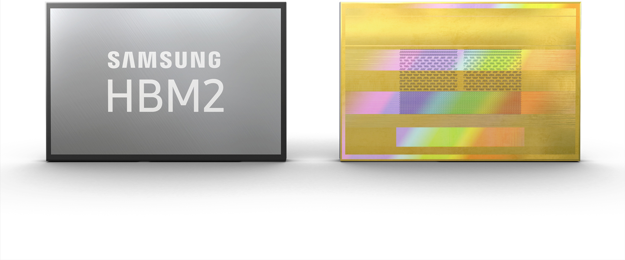
General architecture of Samsung’s new 8 GB HBM2 “Aquabolt” memory is similar to the company’s previous-gen 8 GB HBM2 “Flarebolt” devices: each KGSDs (known good stacked die) is comprised of eight 8-Gb memory ICs (integrated circuits) interconnected using TSVs (through silicon vias) in an 8-Hi stack configuration. Every KGSD features a 1024-bit bus and with a 2.4 Gbps per pin data rate, it can offer up to 307.2 GB/s of memory bandwidth per stack.
| Samsung's HBM2 Memory Comparison | |||||||
| Aquabolt | Flarebolt | ||||||
| Total Capacity | 8 GB | 8 GB | 4 GB | 8 GB | 4 GB | ||
| Bandwidth Per Pin | 2.4 Gb/s | 2 Gb/s | 2 Gb/s | 1.6 Gb/s | 1.6 Gb/s | ||
| Number of DRAM ICs per Stack | 8 | 8 | 4 | 8 | 4 | ||
| DRAM IC Process Technology | 20 nm | ||||||
| Effective Bus Width | 1024-bit | ||||||
| Voltage | 1.2 V | 1.35 V | 1.2 V | ||||
| Bandwidth per Stack | 307.2 GB/s | 256 GB/s | 204.8 GB/s | ||||
When JEDEC published the HBM2 specification about two years ago, the spec only discussed three different speed bins for this type of memory —1 Gbps, 1.6 Gbps and 2.0 Gbps at 1.2 V for core and I/O — in context of timing parameters. Manufacturers are free to offer other speed bins and then developers of actual products can clock HBM2 memory in accordance with their own requirements for performance and power consumption. Meanwhile, standard HBM2 packages are offered with 1.6 Gbps and 2.0 Gbps speed bins (their actual clocks are 800 MHz and 1 GHz, respectively). It is noteworthy that to hit 2 Gbps, Samsung had to increase HBM2 voltages to 1.35 V, which is beyond what the spec allows, but so are realities of mass production.
Samsung’s new Aquabolt products operate at 2.4 Gbps, which is higher than the standard was designed for. Meanwhile, it seems that all the other parameters of the new HBM2 “Aquabolt” memory are perfectly within the spec. Moreover, Samsung’s new memory even lowers its voltage back to 1.2 V as a result of internal optimizations.
To increase actual memory frequency to 1.2 GHz and decrease voltage to 1.2 V at the same time, Samsung had to apply a new method to reduce collateral clock interference between the 5000+ TSVs. Samsung says that to lower the clock skew it had to decrease the deviation of data transfer speeds among the TSVs, but does not go beyond that. In addition, the company increased the number of thermal bumps between the DRAM dies to distribute heat more evenly across each KGSD and thus better dissipate it. Finally, Samsung’s Aquabolt HBM2 products feature an additional protective layer at the bottom to increase the physical strength of the package. It is unknown whether the strengthening had an impact on mechanical characteristics of KGSDs, but this is a possibility.
Makers of memory usually announce mass production of new DRAMs after they complete production the first batch, so the HBM2 Aquabolt memory from Samsung might already exist in more or less mass quantities. Now, it is up to Samsung’s partners to use the new KGSDs in their products.
It is noteworthy that SK Hynix also has 2.4 Gbps HBM2 chips slated for Q1 availability in its product catalog. It is up to SK Hynix to make appropriate announcements, but it looks like Samsung is not going to be alone with fast HBM2 packages in the coming months.
Related Reading:
- Samsung Increases Production Volumes of 8 GB HBM2 Chips Due to Growing Demand
- JEDEC Publishes HBM2 Specification as Samsung Begins Mass Production of Chips
- SK Hynix: Customers Willing to Pay 2.5 Times More for HBM2 Memory
- Hot Chips 2016: Memory Vendors Discuss Ideas for Future Memory Tech - DDR5, Cheap HBM, & More


Source: Samsung


17 Comments
View All Comments
btb - Friday, January 12, 2018 - link
Although it would certainly be great for graphics, I was thinking more along the lines of wether it could be used as a complete replacement for regular DDR4 memory. So we could get rid of the dimm slots altogether and just have 32GB ram sitting on top of the CPU.MrSpadge - Friday, January 12, 2018 - link
"On top" is very problematic for a high performance chip, as the chip would heat the HBM directly instead of the heat sink. This would be unhealthy for the memory and present a huge added thermal resistance for the CPU and hence drive its temperature up (given similar cooling).HBM can be added besides the HPC chip, though, as others have already commented. There are at least 3 issues with that:
- Look at current DRAM frequency scaling. There's not much benefit in higher bandwidth. Which makes sense in the way that the current CPUs are well balanced designs and not starved for bandwidth. Sure, more helps a little bit here and there, but a single HBM stack would already suffice.
- Capacity lock-in. Who are you to dictate everyone's going to be fine with x GB of memory? They could offer some variation with 1 to 8-Hi stacks, but that's not much capacity and they'd create seperate SKUs for all those capacity points (not good for the manufacturer, as they'll overproduce more CPUs which turn out to sell worse than anticipated). And look at it from your side: would you want to "throw away" your probably expensive CPU everytime you want/need more memory?
- Cost: rumor puts a current high performance HBM2 stack at 80$. Sounds excessive but probably includes the relatively expensive packaging and sub-optimal yields. add some vendor margin and Imagine adding 4 of these to a CPU - suddenly it costs 400$ more. That's a tough pill to swallow and way above DDR4 pricing.
SunnyNW - Friday, January 12, 2018 - link
It is alwasy suggested to put the memory on top of the cpu (or gpu) die which of course leads to heat issues. Why not put the cpu on top of the memory?mkozakewich - Friday, January 12, 2018 - link
The board needs the CPU, the CPU needs the memory. If you wanted to put the CPU on top of the memory, you'd need to route everything through the memory to the motherboard, which would be kind of weird and probably pretty expensive.0ldman79 - Saturday, January 13, 2018 - link
The problem is that the quad Core ix series pretty well tops out around 20GBps. Anything below that slows the CPU down, anything much above that isn't used.Now once you start adding more cores and improving the memory controller that's different, but right now DDR4 is feeding it quite well.
There's a benchmark from a couple of years ago that shows this. The numbers may have increased a bit, but we're still not going to see a huge improvement going from 20GBps to 100GBps bandwidth on this architecture.
Zan Lynx - Monday, January 15, 2018 - link
One of the very nice things about putting the CPU and GPU on the same RAM, even if the CPU does not need that bandwidth, is that there is never a need to copy the data. It is just there in RAM available for either processor to use.ktraj1@gmail.com - Thursday, June 28, 2018 - link
What is the formula and explanation that you get these values above?307.2 GB/s 256 GB/s 204.8 GB/s
I know for IOPs etc.... but this one I am not sure.