TSMC: N7+ EUV Process Technology in High Volume, 6nm (N6) Coming Soon
by Anton Shilov on October 8, 2019 2:00 PM EST
TSMC announced on Monday that its customers have started shipping products based on chips made by TSMC using its N7+ (2nd Generation 7 nm with EUV) process technology that uses extreme ultraviolet lithography (EUVL) for up to four layers. The company also said that its clients are on track to tape out chips to be made using N6 node next year.
When compared to N7 (1st Generation 7 nm) that solely relies on deep ultraviolet lithography, TSMC lists its N7+ process as providing a 15% to 20% higher transistor density as well as 10% lower power consumption at the same complexity and frequency. Furthermore, after less than two quarters in production, TSMC is stating that N7+ now matches N7’s yields, which has been used for over a year now.
Use of EUVL enables TSMC to reduce usage of multipatterning technologies when printing highly complex circuits. This also means that TSMC’s EUV tools can offer output power of greater than 250 watts for day-to-day operations while reaching target goals for availability.
| Advertised PPA Improvements of New Process Technologies Data announced by companies during conference calls, press briefings and in press releases |
|||||||||
| TSMC | |||||||||
| 16FF+ vs 20SOC |
10FF vs 16FF+ |
7FF vs 16FF+ |
7FF vs 10FF |
7FF+ vs 7FF |
6FF vs 7FF |
5FF vs 7FF |
|||
| Power | 60% | 40% | 60% | <40% | 10% | ? | 20% | ||
| Performance | 40% | 20% | 30% | ? | same (?) | ? | 15% | ||
| Area Reduction | none | >50% | 70% | >37% | ~17% | 18% | 45% | ||
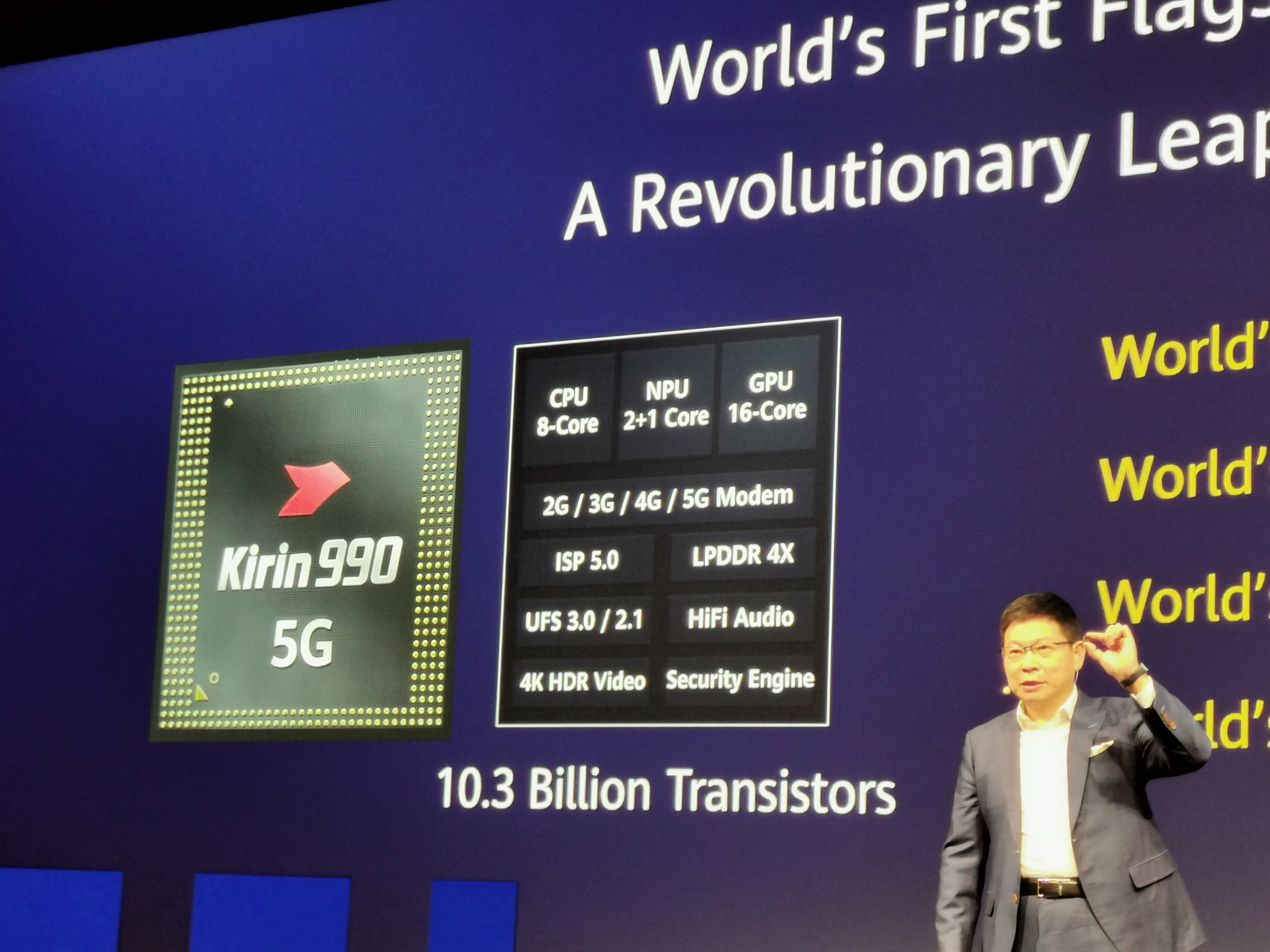
At present, TSMC uses N7+ to produce chips for multiple customers. The most prominent customer of N7+ is Huawei's Hisilicon with the Kirin 990 5G.
TSMC is on track to start risk production of semiconductors using its N6 process technology in the first quarter of 2020 and initiate high-volume production using this node by the end of next year. TSMC’s N6 is a further development of N7 that offers 18% higher transistor density, uses EUVL for up to five layers and enables designers of chips to re-use the same design ecosystem (e.g., tools, IP, etc.), which lowers development costs. By contrast, N7+ uses different design rules, but also provides more benefits than N6 when compared to N7.
Related Reading
- TSMC Announces Performance-Enhanced 7nm & 5nm Process Technologies
- TSMC: Most 7nm Clients Will Transition to 6nm
- TSMC Reveals 6 nm Process Technology: 7 nm with Higher Transistor Density
- TSMC’s 5nm EUV Making Progress: PDK, DRM, EDA Tools, 3rd Party IP Ready
- TSMC: 7nm Now Biggest Share of Revenue
- TSMC: First 7nm EUV Chips Taped Out, 5nm Risk Production in Q2 2019
- TSMC Details 5 nm Process Tech: Aggressive Scaling, But Thin Power and Performance Gains
Source: TSMC


27 Comments
View All Comments
FreckledTrout - Thursday, October 10, 2019 - link
I was replying to you about the process node and the fact you thought Anton was wrong. Anton was not wrong is what i'm saying. As far as Apple I have no idea but I highly suspect they are on 7nm not the 7nm+ process.melgross - Wednesday, October 9, 2019 - link
Apparently, Apple chose the N7 Pro second generation process instead. Both have their advantages.Anymoore - Tuesday, October 8, 2019 - link
I have to wonder if 7nm+ uses this: https://patents.google.com/patent/US9091930B2/enThey have continued the application at USPTO as well.
It would increase the die size as was seen with Huawei Kirin 990 5G.
Oberoth - Wednesday, October 9, 2019 - link
Is TSMC's 6nm sometimes referred to as 5nm because what was all this news about?https://www.techpowerup.com/259536/tsmc-to-begin-m...
levizx - Thursday, October 10, 2019 - link
No. 5nm already entered risk production months ago.FreckledTrout - Thursday, October 10, 2019 - link
The 5nm node is going to be the next real full node change. This is where the magic begins in my opinion. Once we get most features at 5nm we are taking transistor densities that can have CPU and GPU's all in one chip or chiplets on the same package with very little sacrifices. I suspect the dedicated GPU market to retract a ton once we have proper 5nm APU's.Raqia - Thursday, October 10, 2019 - link
Looking forward to that too as GPUs at the 7nm process are already full fledged and pack very interesting features not found on high power envelope parts:https://www.highperformancegraphics.org/wp-content...
Memory bandwidth will have to go up from the roughly ~30 GB/s on 2x 32bit channels found today on most high end SoCs to support that additional compute at 5nm. There is a rumored move to LPDDR5 shortly and there have been 2x 64bit channel configurations such as on the Snapdragon 805 in the past which will help, and the much higher densities of this process will also allow for much larger caches on die to hide low DRAM bandwidth and latencies better.