Where are my GAA-FETs? TSMC to Stay with FinFET for 3nm
by Dr. Ian Cutress on August 26, 2020 12:00 PM EST
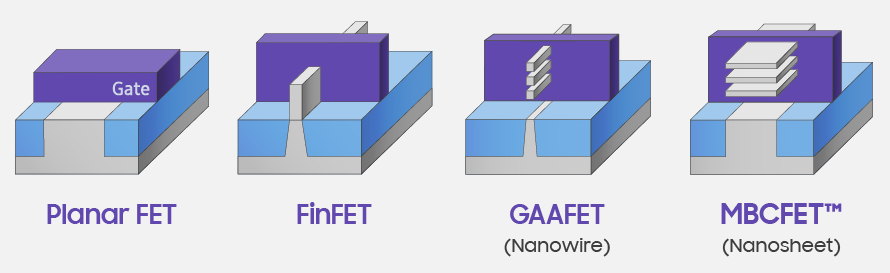
As we passed that 22nm to 16nm barrier, almost all the major semiconductor fabrication companies on the leading edge transitioned from planar transistors to FinFET transistors. The benefits of FinFET were numerous, including better drive currents and lower leakage, better scalability, faster switching times, and an overall better transistor of choice for semiconductor logic. With FinFETs, and multiple rounds of improvements, the technology has scaled from Intel’s first 22nm products down to the 5nm products we will see from TSMC’s partners this year.
As expected, at some point the ability to scale a FinFET will become prohibitive, and new technologies will be needed to help continue the scaling. Research on post-FinFET transistor technology has been progressing at a break-neck pace, and most attention has been moved into ‘Gate-All-Around’ technology, which lifts the channel and allows the channel width to scale as needed for the type of transistor in use. GAA-FETs offer significant advantages when it comes to transistor performance control – for most FinFET processes, foundries can offer several designs based on voltage and performance, but GAA-FET designs turn those discrete options into something more continuous. You might see these referred to as nanosheets, or nanowires.
From Samsung
As is perhaps to be expected, GAA-FET designs (and layered GAA-FETs) are more complex to build than FinFETs or planar transistors. The first GAA-FET demonstration was in 1986, and in 2006 a 3nm implementation was demonstrated. However, building it in a lab compared to building it at scale as part of a foundry process available to customers is a different scale of complexity. At a number of technical semiconductor conferences through 2018 and 2019, a number of design companies and foundry offerings have discussed GAA-FET or similar designs as part of their upcoming portfolio.
Most notably, Intel has mentioned that they will start using it within the next 5 years, which would put it around its 5nm-3nm node technologies.
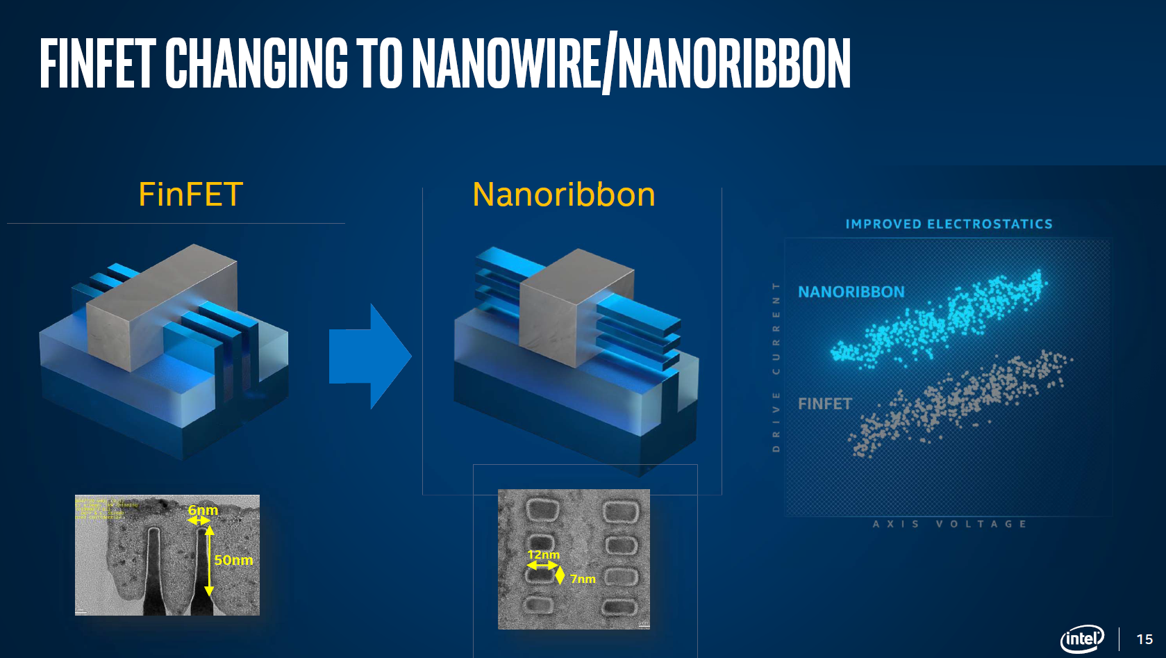
Intel
Samsung has announced its intention to deliver its version, known as MBC-FETs, as part of its 3nm process node, expected to be in volume manufacturing by late 2021. In May 2019, the company released a statement that the first v0.1 version of its 3GAE PDK was ready for customers. Over a year later, we would expect this to be on track – the 2020 version of Samsung’s Foundry Forum, which was delayed due to COVID, should be happening later this year.

Samsung
As these sorts of transistors grow in use, we expect the range of sheet widths available to increase, as well as the number of stacked layers in a GAA design. CEA-Leti this year, at the 2020 Symposia on VLSI Technology and Circuits, demonstrated a 7-layer GAA-FET using nanosheets specifically for high-performance computing.
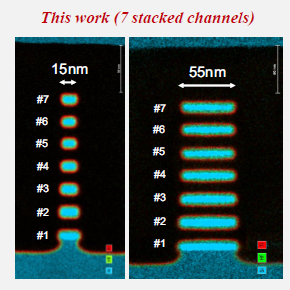
CEA-Leti
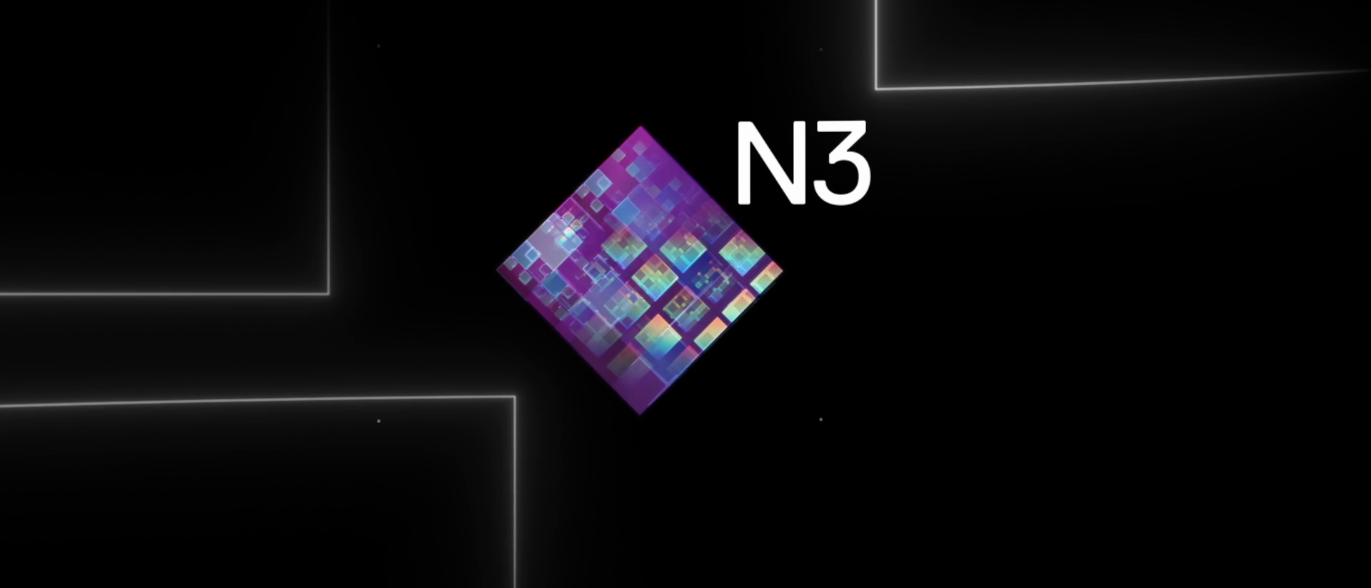
So what has happened with TSMC? As part of the Technology Symposium, it has stated that for its 3nm process technology it will remain with FinFETs. The company states that it has enabled a significant update to its FinFET technology to allow performance and leakage scaling through another iteration of its process node technology. TSMC’s N3 will use an extended and improved version on FinFET in order to extract additional PPA - up to 50% performance gain, up to 30% power reduction, and 1.7x density gain over N5. TSMC stated the predictability of FinFETs will help enable the company deliver the technology on an approved timescale.
This last statement is more than telling – if the development of FinFETs, now on its 3rd/4th/5th generation (depending on the foundry), has enabled a level of comfort and predictability that a first generation of GAA-FET cannot provide, then in order to satisfy its big customers (almost all leading-edge logic silicon), it has to keep to its cadence. That being said, there could be a chance for TSMC to offer GAA-FETs on different versions of its 3nm nodes in the future if it wishes, however the company has not made any public statements at this time to this effect, compared to Intel and Samsung.
As always with these technologies, the goal is to scale and bring some reality to wherever Moore’s Law is going. TSMC’s customers will have to wait until later to see if GAA-FETs can bring a more optimized flavor of performance to the table.
Related Reading
- TSMC Details 3nm Process Technology: Full Node Scaling for 2H22 Volume Production
- TSMC To Build 5nm Fab In Arizona, Set To Come Online In 2024
- TSMC & Broadcom Develop 1,700 mm2 CoWoS Interposer: 2X Larger Than Reticles
- TSMC Boosts CapEx by $1 Billion, Expects N5 Node to Be Major Success
- Early TSMC 5nm Test Chip Yields 80%, HVM Coming in H1 2020
- TSMC: 5nm on Track for Q2 2020 HVM, Will Ramp Faster Than 7nm
- TSMC: N7+ EUV Process Technology in High Volume, 6nm (N6) Coming Soon


37 Comments
View All Comments
RedOnlyFan - Thursday, August 27, 2020 - link
What does tsmc actually mean when they market "5nm" or "2nm", transistor gate lengths?How are they doing "5nm" or "2nm" with DUV?
How many layers euv are they using.. That should be confidential.. Any guesses?
Ian maybe you can enlighten us here.
edzieba - Thursday, August 27, 2020 - link
The big three scaling technologies as we enter the single-digit-nm realm are:- EUV for patterning with reduced numbe rof multi-paterning steps (EUV multi-patterning will rear its head soon enough though)
- Cobalt as a replacement for Copper in lower metal layers (and ascending to higher layers as scales reduce)
- Switching from monolithic fins to perforated things (nanowires/nanosheets).
Intel started by tackling Cobalt first and leaving others to work the bugs out of EUV (mainly isues with the masks and pellicles, as yet unresolved and mostly worked around by significantly reducing the mask life). TSMC and Samsung aimed at EUV first, with TSMC being more gung-ho about getting /some/ EUV in their process even if only for the lowest hanging fruit and Samsung still more tentative. As scales reduce, Intel will need to scale up EUV, and TSMC & Samsung will need to get Cobalt (or another metal, but Cobalt is the least-worst option) into their metal layers, and everyone will need new gate topologies. How well they do getting everything together depends on how much knowledge transfer occurs: Intel may bizzarely be best placed here. They expected EUV to be as hard to implement as it has turned out to be, but expected Cobalt to be much easier than it turned out to be. However, resolving EUV issues is less down to the fabs themselves, and more by ASML and other suppliers who will happily sell solutions to Intel as they do everyone else. But the solutions to getting Cobalt onto the dies reliably and dealing with differential thermal expansion (as killed the 'original' 10nm) remain sitting inside the heads of Intel engineers at the moment.
Tomatotech - Thursday, August 27, 2020 - link
PlanarFET, yes, it's layering. FinFET, yes, make it via more layering. GAAFET.... eh how do they physically make it? Does each nanowire involve stages of laying down material, then laying down the wire, then laying down more material, then laying down another wire on top?Suddenly a transistor has gone from maybe 3 layer to maybe 30+ layers of material, or am I getting the manufacturing process completely wrong?
Spunjji - Thursday, August 27, 2020 - link
I'd really like an explainer on this, too!edzieba - Thursday, August 27, 2020 - link
The 'layers' that will eventually form the wires/ribbons are laid down, a 'fin' is etched, and then additional etching 'side cuts' the gaps between the layers to leave the wires/ribbons, which are than filled in as the gate is deposited.lukedotlol - Tuesday, September 8, 2020 - link
Interesting Gate-All-Around chip recently filed for patentby IBM https://uspto.report/patent/app/20200266060
Oberoth - Wednesday, December 16, 2020 - link
Any update to this?I wonder if there is any chance that Intel's GAA team is totally separate and could mean it will be ready much faster (ie on time) than waiting for 10nm to work properly then waiting for 7nm to working properly then in a few years after that bringing it to market?