A Broadwell Retrospective Review in 2020: Is eDRAM Still Worth It?
by Dr. Ian Cutress on November 2, 2020 11:00 AM EST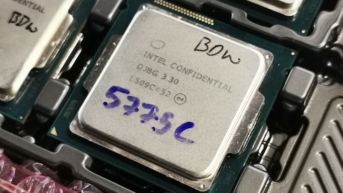
Intel’s first foray into 14nm was with its Broadwell product portfolio. It launched into the mobile market with a variety of products, however the desktop offering in 2015 was extremely limited - only two socketed desktop processors ever made it to retail, and in limited quantities. This is despite users waiting for a strong 14nm update to Haswell, but also because of the way Intel built the chip. Alongside the processor was 128 MB of eDRAM, a sort of additional cache between the CPU and the main memory. It caused quite a stir, and we’re retesting the hardware in 2020 to see if the concept of eDRAM is still worth the effort.
eDRAM: The Savior
In recent years, Intel has pushed hard its infamous ‘Pyramid of Optane’, designed to showcase the tradeoff between small amounts of cache memory close to the CPU being low latency, out to the large offline storage offered for at a significant ping time. When a processor requires data and instructions, it navigates this hierarchy, with the goal to have as much of what is required as close to the CPU (and therefore as fast) as possible.
Traditional modern x86 processors contain three levels of caches, each growing in size and latency, before reaching main memory, and then out to storage. What eDRAM does is add a fourth layer between the last L3 cache on the processor. Whereas the L3 is measured in single digit megabytes, the eDRAM is in the 10s-100s of megabytes, and DRAM measures in gigabytes. Whereas the L3 cache is located on the processor die and low latency, the eDRAM is slightly higher latency, and the main memory is on modules outside the processor socket at the highest latency. Intel enabled an ‘eDRAM’ layer as a separate piece of silicon with the processor package, up to 128 MiB, offering latency and bandwidth between the L3 and main memory.
This piece of silicon was built on Intel’s 22nm IO manufacturing process, rather than 22nm SoC or 14nm, due to Intel’s ability to drive higher 22nm frequencies at the time.

By keeping the eDRAM as a separate piece of silicon, it allowed Intel to adjust stock levels based on demand – if the product failed, there would still be plenty of smaller CPU die for packaging. Even today, processors made with extra eDRAM use the same die as seen back in 2013-2015, showing the longevity of the product. The first eDRAM products were mobile under the 22nm Haswell microarchitecture, but Broadwell saw it come to desktop.
On the Broadwell processors, this resulted in a memory access layer with the following performance:
| Broadwell Cache Structure | ||||
| AnandTech | Size | Type | Latency | Bandwidth |
| L1 Cache | 32 KiB / core | Private | 4-cycle | 880 GiB/s |
| L2 Cache | 256 KiB / core | Private | 12-cycle | 350 GiB/s |
| L3 Cache | 6 MiB | Shared | 26-50 cycle | 175 GiB/s |
| eDRAM | 128 MiB | Shared | < 150 cycle | 50 GiB/s |
| DDR3-1600 | Up to 16 GiB | Shared | 200+ cycle | 25.6 GiB/s |
The simplistic view of this eDRAM was as a ‘level 4’ cache layer – this is ultimately how it was described to us at the time, with the eDRAM layer acting as a victim cache accepting L3 evictions but enabled through a shadow tag system accessed through the L3. Data needed from the eDRAM would have to be moved back into L3 before going anywhere else, including the graphics or the other IO or main memory. In order to do this, these shadow tags required approximately 0.5 MiB/core of the L3 cache, reducing the L3 usefulness in exchange for lower latency extending out to 128 MiB. This is why Broadwell only had 1.5 MiB/core of L3 cache, rather than the full 2.0 MiB/core that the die shot suggested it should have.
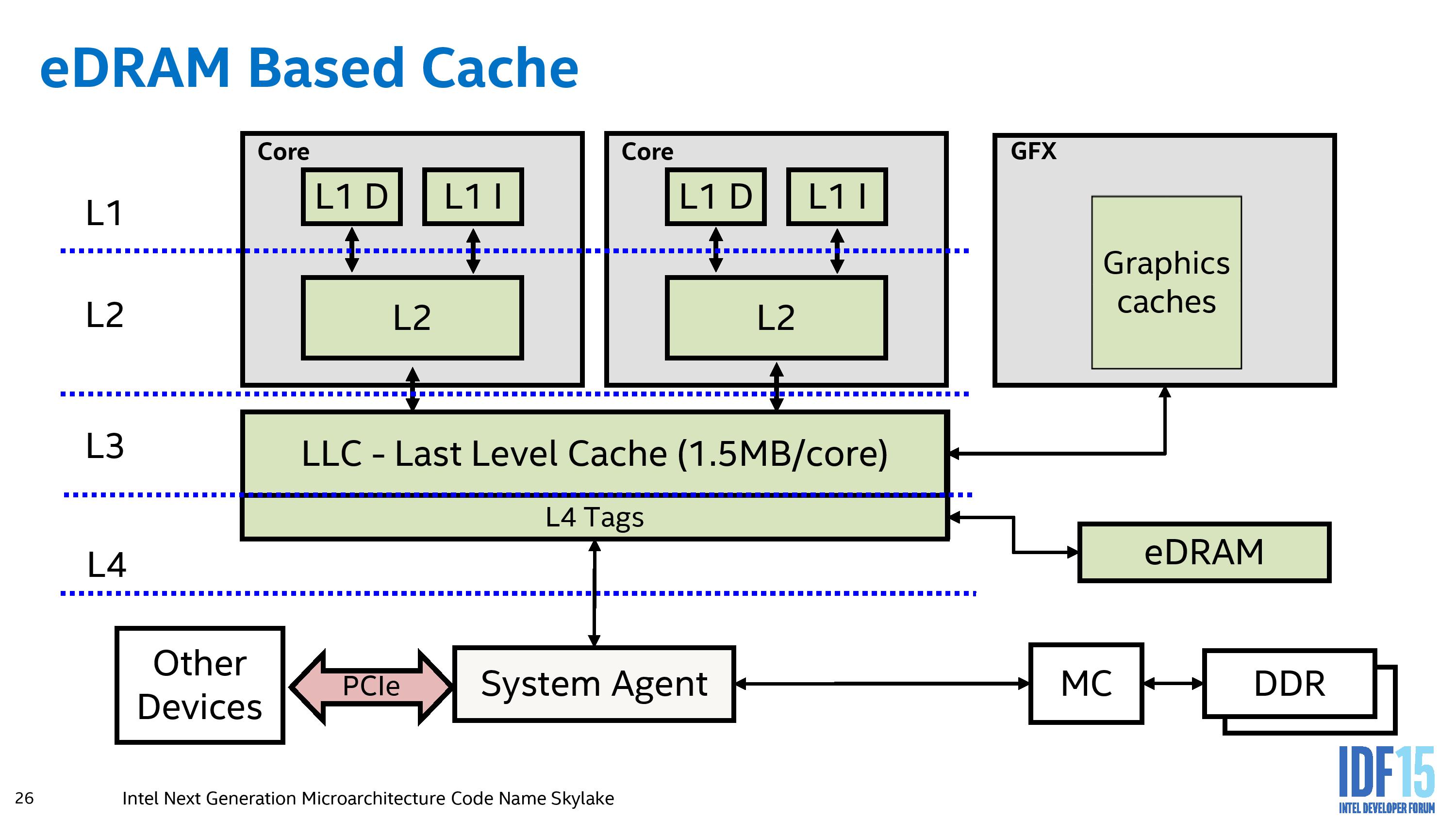
Haswell/Broadwell eDRAM Layout
The eDRAM could be dynamically split on the fly for CPU or GPU requests, allowing it to be used in CPU-only mode when the integrated graphics are not in use, or full for the GPU when texture caching is required. The interface was described to us at the time as a narrow double-pumped serial interface capable of 50 GiB/s bi-directional bandwidth (100 GiB/s aggregate), running at a peak 1.6 GHz.
In this configuration, in combination with the graphics drivers, allowed for more granular control of the eDRAM, suggesting that the system could pull from both the eDRAM and the DDR memory simultaneously, potentially giving a peak memory bandwidth of 75.6 GiB/s, at a time when mid-range graphics cards such as the GT650M had a bandwidth around 80 GiB/s.
The second generation of the eDRAM design, as found in Skylake and future processors, moved the eDRAM out of the purview of the L3 cache, and enabled it as a purely transparent buffer between the system agent and the main DRAM memory controller, making it invisible to CPU/GPU accesses or IO accesses. This allows the cache to be accessed by all DRAM requests, enabling full coherency (although the drivers still allow it to be bypassed for textures larger than the eDRAM size), as well as removing the 0.5 MiB/core L3 cache reduction for shadow tags.
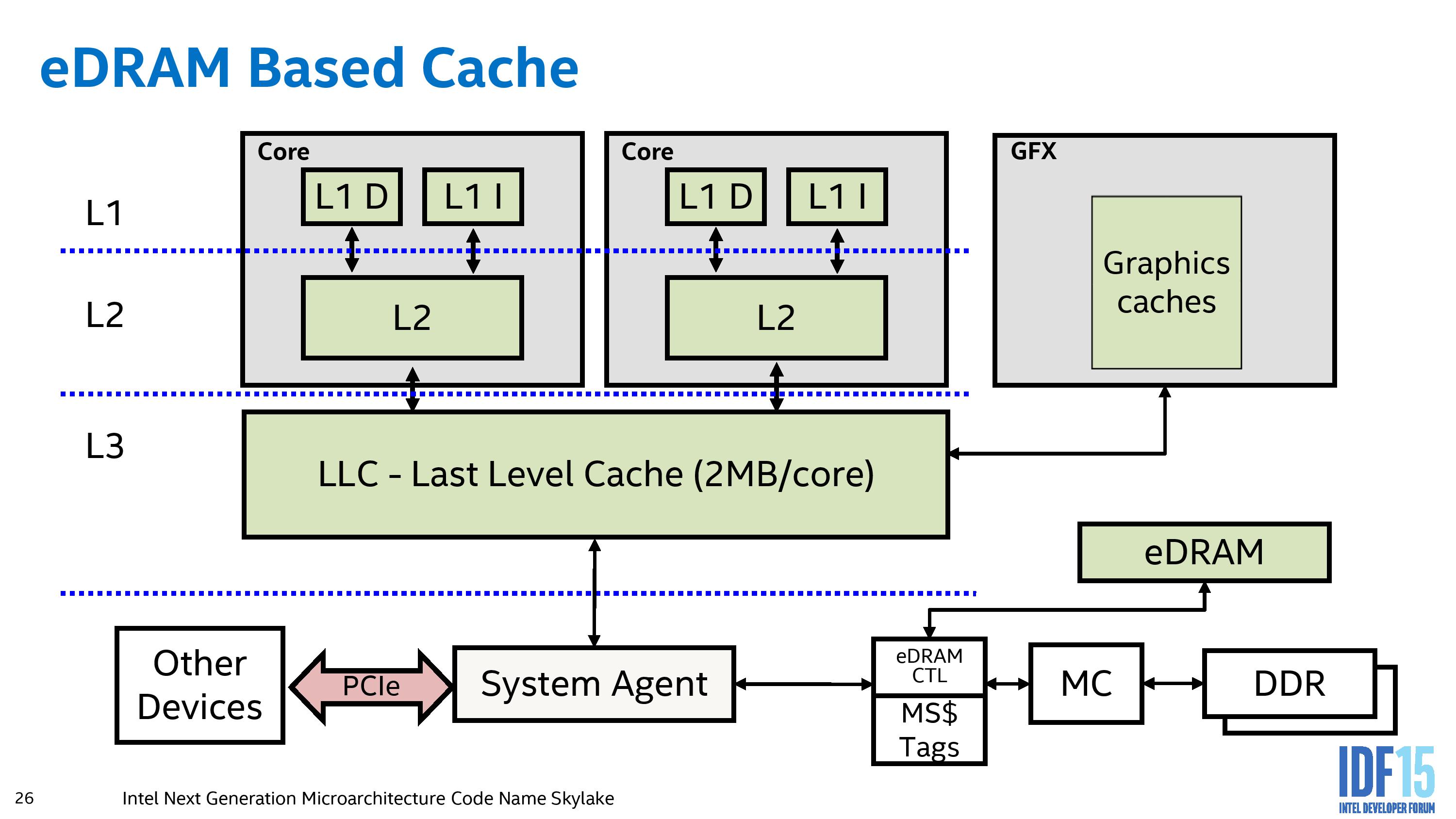
Skylake-and-beyond eDRAM Layout
There are arguments to be made about whether the eDRAM as an L4 victim cache or as a transparent buffer to DRAM is the correct direction to go – as a victim cache, Intel stated it allowed a cache hit rate over 95%, however in a number of scenarios in order to get the best performance it required software intervention, and a lot of software was not aware of such a configuration. As a buffer, it enabled seamless integration that all software can take advantage of, but it is not necessarily as optimizable as an L4 victim cache.
‘Go Big or Go Home’
For Broadwell’s eDRAM products, Intel enabled a 128 MiB implementation, quadruple that found on Xbox One silicon at the time. At the time, Intel said that a 32 MiB eDRAM L4 victim cache enabled substantial hit rates, but the company wanted the design to be futureproof as well as a long-term option in Intel’s product stack, so it was doubled, and doubled again just to be sure. The term was ‘go big or go home’, and in our initial review of the first Broadwell eDRAM products, Anand noted that it was very rare to see Intel be so ‘liberal’ with die area.
The eDRAM silicon was built on the 22nm SoC process, as mentioned, one node behind Intel’s leading edge CPU designs. The 128 MiB design came in at a die size of ~77 mm2, contributing to over a third of the total die area used in the 14nm Broadwell Iris Pro quad-core processor package (182mm2 + 77mm2 = 259 mm2).
In the subsequent next generation Skylake generation, eDRAM models with 64 MiB were also offered.
Under certain constraints, the system could save power by disabling the main memory controller entirely if all the data required over a period of time is available in the eDRAM. As part of the initial Broadwell launch, Intel described the extra power consumption of the eDRAM as under 1 watt at idle, moving up to a peak of 5 watts when operating at full bandwidth. Ultimately this means that at a chip level, less power is available to the cores should it be needed, but the trade-off will be better performance in memory limited scenarios. The power is meant to be tracked by the on-die PCU, or Power Control Unit, that can shift power budget between the CPU, GPU, eDRAM, as needed by performance counters or thermals.
As part of this review, we are able to give at least some insights into this number. In our testing, we saw idle package power numbers for the following processors:
- Core i7-4790S (22nm Haswell 4 core 6 MiB L3): 6.01 W
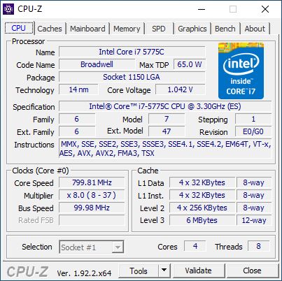
- Core i7-5775C (14nm Broadwell 4 core 6 MiB L3 + 128 MiB eDRAM) 9.71 W
- Core i7-6700K (14nm Skylake 4 core 8 MiB L3): 6.46 W
These numbers would suggest that the effect of the eDRAM, at idle, is more akin to 3.3-3.7 watts, not the sub 1-watt that Intel suggested. Perhaps that sub 1-watt value was more for mobile processors? When running at a steady-state full load, the processors reported power values of their TDP, which doesn’t enable any insight.
Broadwell’s eDRAM Flop?
Intel had somewhat backed itself into a corner with its Broadwell launch. Due to the delays of Intel’s 14nm process at the time, the company had decided to follow its popular Haswell-based 22nm Core i7-4770K high-end processor with the launch of a higher binned ‘Devil’s Canyon’ processor, the Core i7-4790K. This processor offered +500 MHz, which at the time was a substantial jump in performance, despite the processors being launched 12 months apart.
Devil’s Canyon Review: Intel Core i7-4790K and i5-4690K
Because Broadwell ‘wasn’t ready’, Devil’s Canyon was designed to be a stop-gap measure to appease Intel’s ever-hungry consumers and high-end enthusiasts. From the consumer point of view, Devil’s Canyon was at least a plus, but it gave Intel a significant headache.
By bumping the clock speed of its leading consumer processor by a significant margin, Intel now had a hill to climb – the goal of a new product generation is that it should be better than what came before. By boosting its previous best to be even better, it meant the next generation had to do even more. This is difficult to do when the upcoming process node isn’t working quite right. This meant that in the land of the desktop processor, Intel’s reluctance to launch Broadwell with eDRAM was painful to see, and the company had to change strategy.

Intel almost made Broadwell for desktops a silent launch, with very little fanfare. After the announcement, there was almost zero stock on shelves. At the time, Intel did not sample the processors for review – we were able to obtain units from other sources a few days in advance for our launch day coverage.
The Intel Broadwell Desktop Review: Core i7-5775C and Core i5-5675C Tested (Part 1)
The Intel Broadwell Review Part 2: Overclocking, IPC and Generational Analysis
By launching Broadwell Core i7 as a 65 W processor rather than an 84-88 W processor, it meant that the lower frequency Broadwell wasn’t necessarily a direct comparison to Devil’s Canyon. It came out of the gate with a frequency deficit, however the presence of the eDRAM would enable some very careful wins in memory limited scenarios, and perhaps most importantly, gaming.
Ultimately the stunted launch of desktop Broadwell in June 2nd 2015 was very quickly followed by launch of Skylake on August 5th 2015, and the top Core i7 processor was once again an 88+ watt unit and a true like-for-like competitor to Devil’s Canyon. Skylake also enabled DDR4 in the market, which was a significant upgrade on the memory front.
Unfortunately Intel had another conundrum – the older Broadwell processors, due to the eDRAM, actually offered slightly better gaming performance than Skylake! It was title, resolution, and quality dependent, and some might argue there was only a few percentage points in it, but for those that wanted the best at gaming, Skylake wasn’t necessarily the answer. For pretty much all CPU tasks though, Skylake was the answer.
Broadwell Still Available Today
Ultimately, Intel’s foray into socketed Broadwell processors with eDRAM was a momentary blip in its line of consumer-focused Core products. At the time, the processors were hard to find for sale, and were quickly made old by the arrival of Skylake and DDR4. There were six different Broadwell processors that were socketable, two mainstream Core products and four Xeon E3 parts.
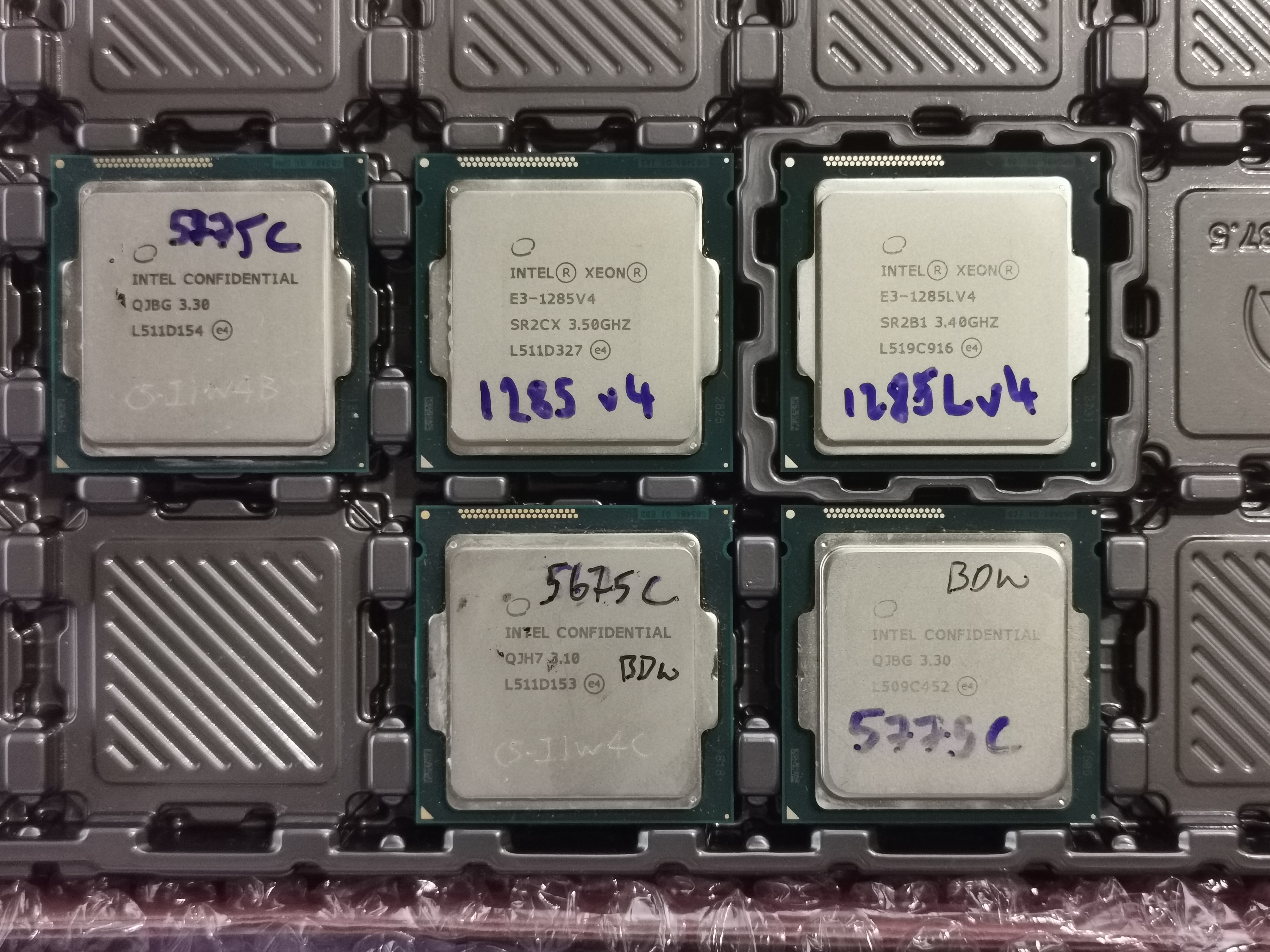
| Intel Broadwell eDRAM Socketable CPUs | ||||||
| AnandTech | Cores Threads |
Base Freq |
Turbo Freq |
IGP | IGP Freq |
TDP |
| Consumer Core | ||||||
| i7-5775C | 4C / 8T | 3300 | 3700 | 48 EUs | 1150 | 65 W |
| i5-5675C * | 4C / 4T | 3100 | 3600 | 48 EUs | 1100 | 65 W |
| * Sometimes listed as Core i7-5675C as some ES had an incorrect CPUID string | ||||||
| Enterprise Xeon E3 v4 | ||||||
| E5-1285 v4 | 4C / 8T | 3500 | 3800 | 48 EUs | 1150 | 95 W |
| E5-1285L v4 | 4C / 8T | 3400 | 3800 | 48 EUs | 1150 | 65 W |
| E3-1270L v4 | 4C / 8T | 3000 | 3600 | - | - | 45 W |
| E3-1265L v4 | 4C / 8T | 2300 | 3300 | 48 EUs | 1050 | 35 W |
We were able to also review three of the Xeons at the time.
The Intel Broadwell Xeon E3 v4 Review: 95W, 65W and 35W with eDRAM
Most of these processors are actually very easy to purchase today. The best place to find them are either on Aliexpress, or eBay, for as little as $104.
Broadwell in 2020
The main highlight of these processors was the high-speed eDRAM, coming up to 50 GiB/s bidirectional, at a time when the DDR3-1600 memory solution in dual channel could only offer 25.6 GiB/s. At some point in the future, it would be expected for the speed of normal DRAM to surpass this bandwidth offered, even if it can’t exactly match that latency.
We actually reached that mark very recently.
- Intel’s best consumer-grade processor is the Intel Core i9-10900K, offering 10 cores up to a peak 5.3 GHz, but most importantly the memory side has official support for DDR4-2933, which in dual channel mode would enable 46.9 GiB/s.
- Current AMD Zen 2 processors have a peak supported frequency of DDR4-3200, which in dual channel mode would enable 51.2 GiB/s bandwidth.
- Intel’s mobile Tiger Lake processors support LPDDR4X-4266, which when fully populated would provide 68.2 GiB/s bandwidth.
- With the introduction of DDR5 set to come in the next couple of years, we are expecting to see DDR5-4800 as a possible entry point. This would enable 38.4 GiB/s per 64-bit channel, or 76.8 GiB/s in a standard consumer configuration.
Perhaps it is difficult to wrap your head around the fact that only in 2020 are we matching bandwidth levels that were enabled back in 2015 by the addition of a simple piece of silicon. It might make you question why Broadwell was the only family of Intel’s socketable processors to get this innovation – all future eDRAM products were all for mobile devices that rely on integrated graphics, despite the benefits observed for discrete graphics configurations.
It should be noted that because eDRAM offers a latency benefit in memory accesses from 6 MiB to 128 MiB, then as we approach the situation where a single core has access to 128 MiB of L3 cache, this benefit would also disappear. For consumer processors, we’re not there quite yet – while Intel processors offer up to 20 MiB (or 24 MiB in upcoming Tiger Lake 8-core processors), AMD’s future Zen 3 processors will offer access to 32 MiB of L3 for each core within a CCX. By that metric, we’re still very far behind.
For this review, because we recently tested Intel’s Tiger Lake quad-core processors and graphics, I wanted to probe exactly where Broadwell will finally sit in the hierarchy of CPU performance and graphics performance. We recently announced a new benchmark and gaming suite, and Broadwell is always one of the interesting products to put on a new test suite.
All integrated gaming tests (as well as gaming tests with an RTX 2080 Ti) will be under the respective game pages.
Pages In This Review
- Analysis and Competition
- Test Setup and #CPUOverload Benchmarks
- Power Consumption
- CPU Tests: Office and Science
- CPU Tests: Simulation
- CPU Tests: Rendering
- CPU Tests: Encoding
- CPU Tests: Legacy and Web Tests
- CPU Tests: Synthetics
- CPU Tests: SPEC
- CPU Tests: Microbenchmarks
- Gaming: Chernobylite
- Gaming: Civilization VI
- Gaming: Deus Ex: MD
- Gaming: Final Fantasy XIV
- Gaming: Final Fantasy XV
- Gaming: World of Tanks
- Gaming: Borderlands 3
- Gaming: F1 2019
- Gaming: Far Cry 5
- Gaming: Gears Tactics
- Gaming: GTA 5
- Gaming: Red Dead Redemption 2
- Gaming: Strange Brigade
- Conclusions and Final Words


120 Comments
View All Comments
brucethemoose - Monday, November 2, 2020 - link
Is HBM2e access latency really lower than DDR4/5?I cant find any timing info or benchmarks, but my understanding is that its lower than GDDR6, which already has much higher latency than DDR4.
PeachNCream - Monday, November 2, 2020 - link
I'd like to say thanks for this review! I really love the look backwards at older hardware in relationship to modern systems. It really shows that in processor power terms that Broadwell/Haswell remain fairly relevant and the impact of eDRAM (or non-impact in various workloads) makes for really interesting reading.brucethemoose - Monday, November 2, 2020 - link
Another possibility: the "Radeon Cache" on an upcoming APU acts as a last level cache for the entire chip, just like Apple (and Qualcomm?) SoCs.Theres no extra packaging costs, no fancy 2nd chip, and it would save power.
Jorgp2 - Monday, November 2, 2020 - link
You do realize that Intel has had that about as long as they've had GPUs on their CPUs right?brucethemoose - Monday, November 2, 2020 - link
You mean the iGPUs share L3?Well, its wasn't a particularly large cache or powerful GPU until Broadwell came around.
Jorgp2 - Tuesday, November 3, 2020 - link
>Well, its wasn't a particularly large cache or powerful GPU until Broadwell came around.Larger than the caches on even AMDs largest GPUs until recently.
Hawaii had a 4MB cache, Vega had a 6MB I believe.
eastcoast_pete - Monday, November 2, 2020 - link
Thanks Ian, great article! Regarding a large, external L4 Cache: any guess on how speed and latency of eDRAM made in more modern silicon would compare with Broadwell's 22 nm one? Let's say if made in Intel's current 14 nm (++ etc)? And, if that'll speed it up enough to make it significantly better than current fast DDR4, would that be a way for Intel to put some "electronic nitrous" on its Tiger Lake and Rocket Lake chips? Because they do need something, or they'll get spanked badly by the new Ryzens.brucethemoose - Monday, November 2, 2020 - link
I'm guessing most of the latency comes from the travel between the chips, not from the speed of the eDRAM itself. So a shrink wouldnt help much, but EMIB might?There is talk of replacing on-chip SRAM in L3 cache with eDRAM, kind of like what IBM already does. So basically, its a size vs speed tradeoff, which is very interesting indeed.
quadibloc - Monday, November 2, 2020 - link
Well, AMD seems to think it was a good idea, given the 128 MB Infinity Cache on their latest graphics cards...Leeea - Monday, November 2, 2020 - link
Close, but not quite the same.AMD has their infinity cache in the GPU die. One piece of silicon for the whole thing. This may have faster I/O and less power consumption.
Intel's eDRAM caches were separate a separate piece of silicon all together.