SK Hynix Announces 176-Layer 3D NAND
by Billy Tallis on December 7, 2020 8:00 AM EST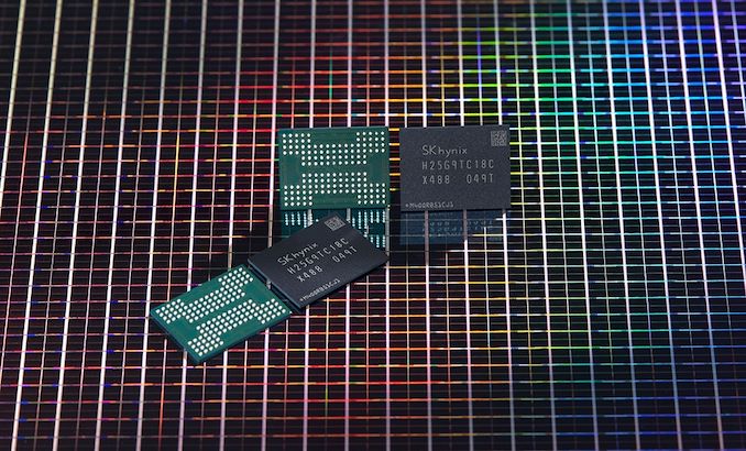
SK hynix has announced their latest generation of 3D NAND, now featuring 176 layers of charge trap flash memory cells. SK hynix is the second NAND manufacturer to reach this layer count, following Micron's announcement that their 176L NAND was starting to ship in Crucial-branded products.
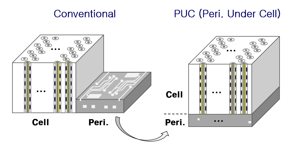
This is SK hynix's third generation to feature their Periphery under Cell (PUC) design to reduce die size by placing peripheral logic under the memory cell array, similar to Intel and Micron's CMOS Under Array design. (SK hynix refers to the combination of this die layout and their charge trap flash cells as "4D NAND".) Changes with this generation include a 35% increase in bit productivity (only slightly less than theoretically possible with the jump from 128 to 176 layers) and a 20% increase in cell read speed. The maximum IO speed between NAND dies and the SSD controller has been increased from 1.2GT/s for their 128L NAND to 1.6GT/s for the 176L NAND.
SK hynix has started sampling a 512Gbit TLC part to SSD controller companies for developing compatible firmware. SK hynix plans to initially use their 176L NAND for mobile products (ie. UFS modules) which will offer 70% faster read speeds and 35% faster write speeds, due to be introduced around the middle of next year. The mobile products will then be followed up by consumer and enterprise SSDs. SK hynix also plans to introduce 1Tbit dies based on their 176L process.
Based on this announcement, it appears that SK hynix will be fairly competitive during the upcoming generation of 3D NAND. They may be running a bit behind Micron's schedule, but Micron has been pursuing an unusually quick transition to 176L after using their 128L generation as a low-volume test vehicle to work out any issues resulting from their switch from floating gate to charge trap cell design. Meanwhile, Intel's 144L NAND should be arriving early next year, and Kioxia/Western Digital 112L NAND is due to show up any day now. Samsung's 128L NAND started shipping a few months ago in the 980 PRO. While they have not officially announced specs for their next generation, it is expected to go into production next spring with a layer count in the neighborhood of 176L, and to be Samsung's first generation to use string stacking—a technique their competitors all had to adopt while layer counts were in the 64-96L range.
Related Reading:
- Micron Announces 176-layer 3D NAND
- SK Hynix to Buy Intel’s NAND Memory Business For $9 Billion
- The Best NVMe SSD for Laptops and Notebooks: SK hynix Gold P31 1TB SSD Reviewed
- Western Digital and Kioxia Announce BiCS5 112-Layer 3D NAND
Source: SK hynix


29 Comments
View All Comments
waterdog - Monday, December 7, 2020 - link
Acme spell checkerTomatotech - Tuesday, December 8, 2020 - link
No, a wily spellchecker.bill.rookard - Monday, December 7, 2020 - link
Wile is a word. You'd have to check grammar to catch that as a mistake. "She used her feminine wiles to lure him into bed."at_clucks - Friday, December 11, 2020 - link
Goes to show spell checkers are not proof readers.Kurosaki - Tuesday, December 8, 2020 - link
Hey, don't be vile.WatcherCK - Monday, December 7, 2020 - link
Is recycling of NAND a thing yet? Even if it is just grinding up the chips and reusing the resulting materials?PixyMisa - Tuesday, December 8, 2020 - link
If you grind up the chips you get sand.Anymoore - Tuesday, December 8, 2020 - link
Now that SK Hynix has bought Intel's NAND, their roadmap definitely needs some clarification.Snowleopard3000 - Wednesday, December 16, 2020 - link
So if I want 1 nvme drive for the os and applications where speed is key and then a second separate nvme for storage, what 2 nvme drives should I be looking at?