Cerebras Unveils Wafer Scale Engine Two (WSE2): 2.6 Trillion Transistors, 100% Yield
by Dr. Ian Cutress on April 20, 2021 2:00 PM EST
The last few years has seen a glut of processors enter the market with the sole purpose of accelerating artificial intelligence and machine learning workloads. Due to the different types of machine learning algorithms possible, these processors are often focused on a few key areas, but one thing limits them all – how big you can make the processor. Two years ago Cerebras unveiled a revolution in silicon design: a processor as big as your head, using as much area on a 12-inch wafer as a rectangular design would allow, built on 16nm, focused on both AI as well as HPC workloads. Today the company is launching its second generation product, built on TSMC 7nm, with more than double the cores and more than double of everything.
Second Generation Wafer Scale Engine
The new processor from Cerebras builds on the first by moving to TSMC’s N7 process. This allows the logic to scale down, as well as to some extent the SRAMs, and now the new chip has 850,000 AI cores on board. Basically almost everything about the new chip is over 2x:
| Cerebras Wafer Scale | |||
| AnandTech | Wafer Scale Engine Gen1 |
Wafer Scale Engine Gen2 |
Increase |
| AI Cores | 400,000 | 850,000 | 2.13x |
| Manufacturing | TSMC 16nm | TSMC 7nm | - |
| Launch Date | August 2019 | Q3 2021 | - |
| Die Size | 46225 mm2 | 46225 mm2 | - |
| Transistors | 1200 billion | 2600 billion | 2.17x |
| (Density) | 25.96 mTr/mm2 | 56.246 mTr/mm2 | 2.17x |
| On-board SRAM | 18 GB | 40 GB | 2.22x |
| Memory Bandwidth | 9 PB/s | 20 PB/s | 2.22x |
| Fabric Bandwidth | 100 Pb/s | 220 Pb/s | 2.22x |
| Cost | $2 million+ | arm+leg | ‽ |
As with the original processor, known as the Wafer Scale Engine (WSE-1), the new WSE-2 features hundreds of thousands of AI cores across a massive 46225 mm2 of silicon. In that space, Cerebras has enabled 2.6 trillion transistors for 850,000 cores - by comparison, the second biggest AI CPU on the market is ~826 mm2, with 0.054 trillion transistors. Cerebras also cites 1000x more onboard memory, with 40 GB of SRAM, compared to 40 MB on the Ampere A100.

Me with Wafer Scale Gen1 - looks the same, but with less than half the cores.
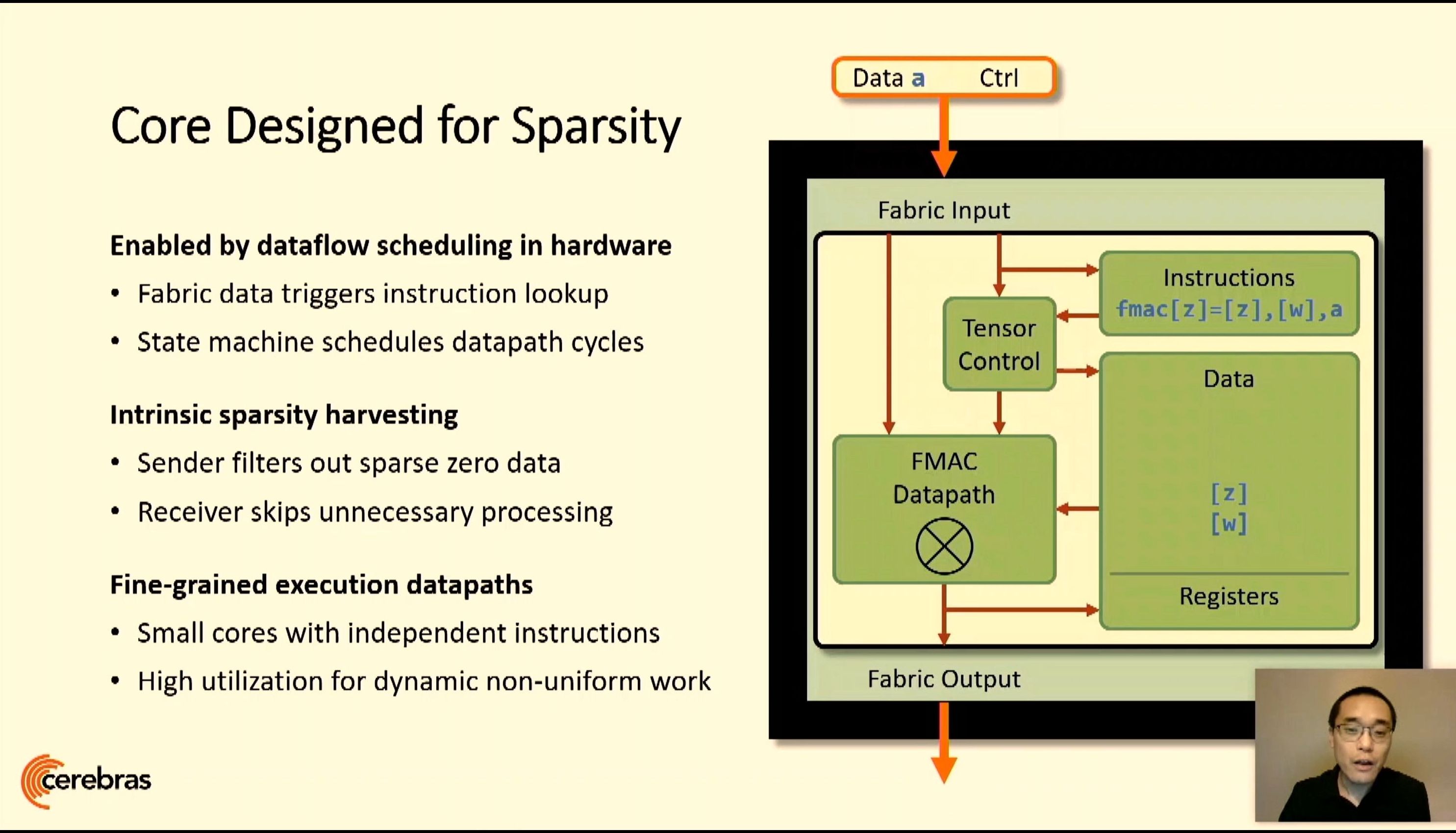
The cores are connected with a 2D Mesh with FMAC datapaths. Cerebras achieves 100% yield by designing a system in which any manufacturing defect can be bypassed – initially Cerebras had 1.5% extra cores to allow for defects, but we’ve since been told this was way too much as TSMC's process is so mature. Cerebras’ goal with WSE is to provide a single platform, designed through innovative patents, that allowed for bigger processors useful in AI calculations but has also been extended into a wider array of HPC workloads.
Building on First Gen WSE
A key to the design is the custom graph compiler, that takes pyTorch or TensorFlow and maps each layer to a physical part of the chip, allowing for asynchronous compute as the data flows through. Having such a large processor means the data never has to go off-die and wait in memory, wasting power, and can continually be moved onto the next stage of the calculation in a pipelined fashion. The compiler and processor are also designed with sparsity in mind, allowing high utilization regardless of batch size, or can enable parameter search algorithms to run simultaneously.
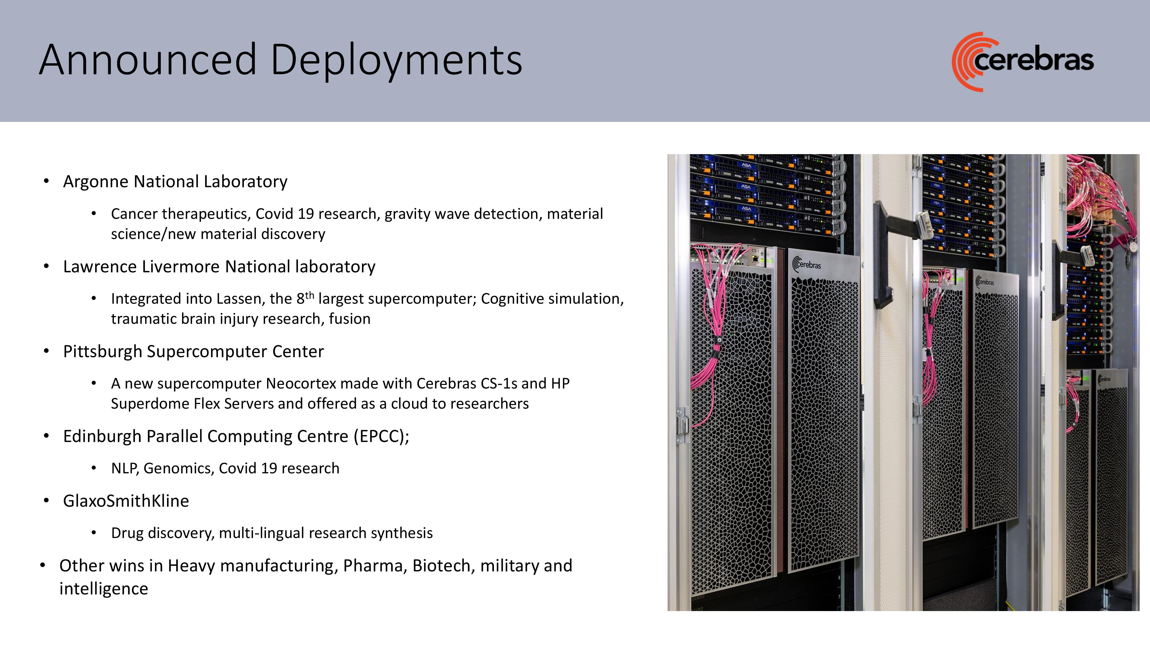
For Cerebras’ first generation WSE is sold as a complete system called CS-1, and the company has several dozen customers with deployed systems up and running, including a number of research laboratories, pharmaceutical companies, biotechnology research, military, and the oil and gas industries. Lawrence Livermore has a CS-1 paired to its 23 PFLOP ‘Lassen’ Supercomputer. Pittsburgh Supercomputer Center purchased two systems with a $5m grant, and these systems are attached to their Neocortex supercomputer, allowing for simultaneous AI and enhanced compute.
Products and Partnerships
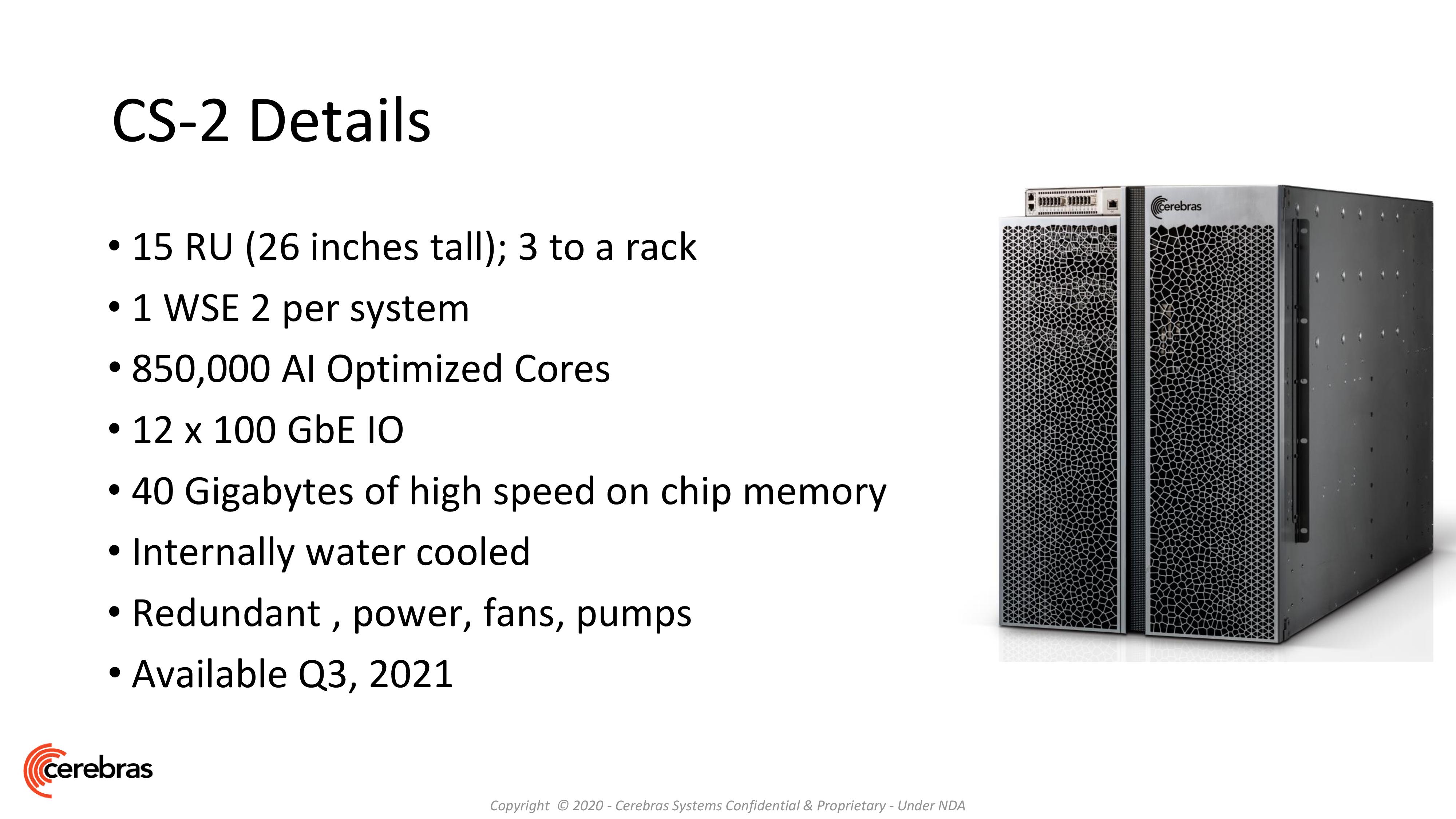
Cerebras sells complete CS-1 systems today as a 15U box that contains one WSE-1 along with 12x100 GbE, twelve 4 kW power supplies (6 redundant, peak power about 23 kW), and deployments at some institutions are paired with HPE’s SuperDome Flex. The new CS-2 system shares this same configuration, albeit with more than double the cores and double the on-board memory, but still within the same power. Compared to other platforms, these processors are arranged vertically inside the 15U design in order to enable ease of access as well as built-in liquid cooling across such a large processor. It should also be noted that those front doors are machined from a single piece of aluminium.
The uniqueness of Cerebras’ design is being able to go beyond the physical manufacturing limits normally presented in manufacturing, known as the reticle limit. Processors are designed with this limit as the maximum size of a chip, as connecting two areas with a cross-reticle connection is difficult. This is part of the secret sauce that Cerebras brings to the table, and the company remains the only one offering a processor on this scale – the same patents that Cerebras developed and were awarded to build these large chips are still in play here, and the second gen WSE will be built into CS-2 systems with a similar design to CS-1 in terms of connectivity and visuals.

The same compiler and software packages with updates enable any customer that has been trialling AI workloads with the first system to use the second at the point at which they deploy one. Cerebras has been working on higher-level implementations to enable customers with standardized TensorFlow and PyTorch models very quick assimilation of their existing GPU code by adding three lines of code and using Cerebras’ graph compiler. The compiler then divides the whole 850,000 cores into segments of each layer that allow for data flow in a pipelined fashion without stalls. The silicon can also be used for multiple networks simultaneously for parameter search.

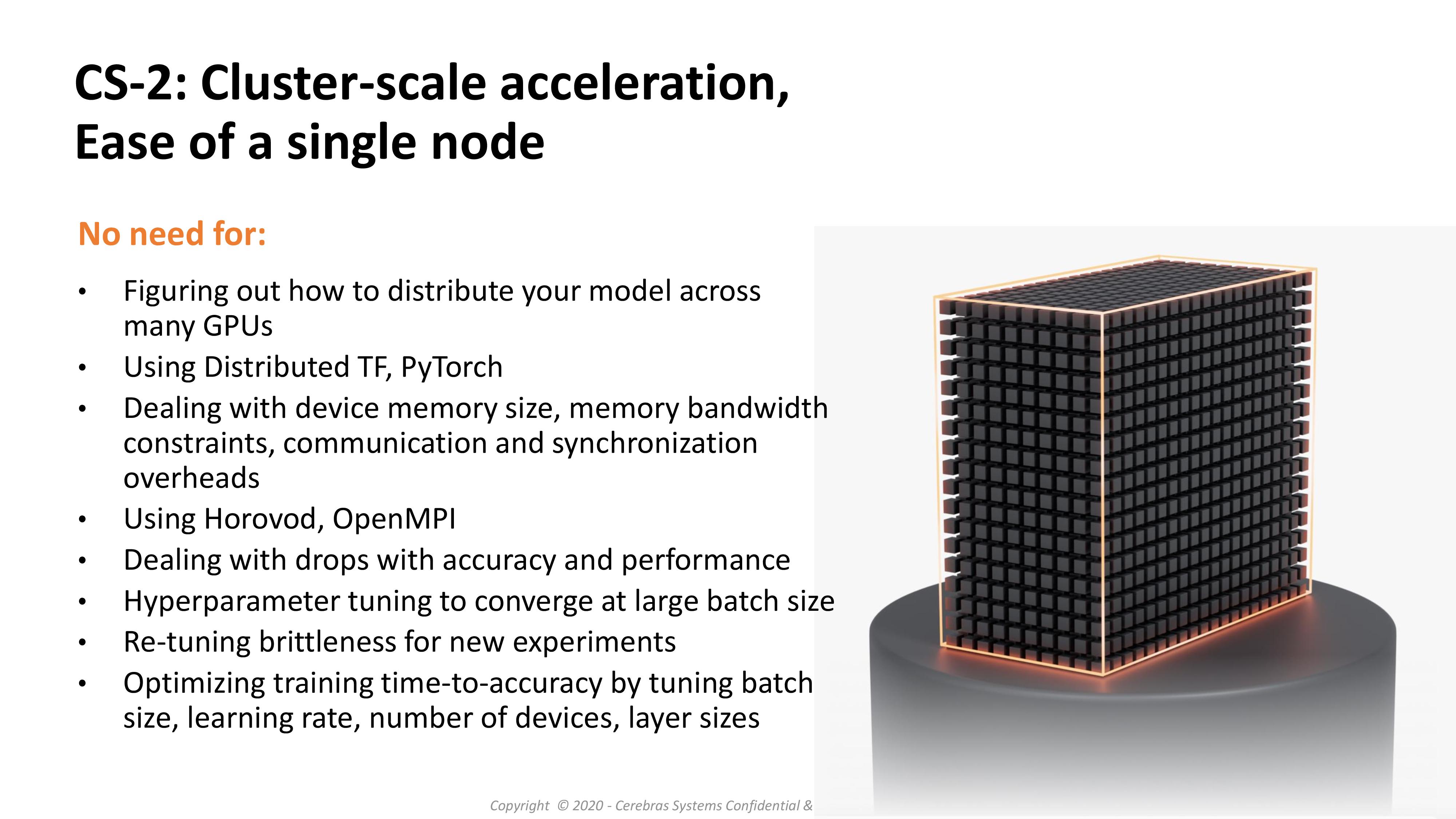
Cerebras states that with having such a large single chip solution means that the barrier to distributed training methods across 100s of AI chips is now so much further away that this excess complication is not needed in most scenarios – to that, we’re seeing CS-1 deployments of single systems attached to supercomputers. However, Cerebras is keen to point out that two CS-2 systems will deliver 1.7 million AI cores in a standard 42U rack, or three systems for 2.55 million in a larger 46U rack (assuming there’s sufficient power for all at once!), replacing a dozen racks of alternative compute hardware. At Hot Chips 2020, Chief Hardware Architect Sean Lie stated that one of Cerebras' key benefits to customers was the ability to enable workload simplification that previously required racks of GPU/TPU but instead can run on a single WSE in a computationally relevant fashion.
As a company, Cerebras has ~300 staff across Toronto, San Diego, Tokyo, and San Francisco. They have dozens of customers already with CS-1 deployed and a number more already trialling CS-2 remotely as they bring up the commercial systems. Beyond AI, Cerebras is getting a lot of interest from typical commercial high performance compute markets, such as oil-and-gas and genomics, due to the flexibility of the chip is enabling fluid dynamics and other compute simulations. Deployments of CS-2 will occur later this year in Q3, and the price has risen from ~$2-3 million to ‘several’ million.

With Godzilla for a size reference
Related Reading
- Cerebras Wafer Scale Engine News: DoE Supercomputer Gets 400,000 AI Cores
- 342 Transistors for Every Person In the World: Cerebras 2nd Gen Wafer Scale Engine Teased
- Cerebras’ Wafer Scale Engine Scores a Sale: $5m Buys Two for PSC
- Hot Chips 2020 Live Blog: Cerebras WSE Programming (3:00pm PT)
- Hot Chips 2019 Live Blog: Cerebras' 1.2 Trillion Transistor Deep Learning Processor


136 Comments
View All Comments
Rudde - Tuesday, April 20, 2021 - link
There are different transistor libraries. The high density libraries pack more transistors into a smaller area, while the high performance libraries enable a higher frequency. Phone SoCs use density, as they have neither the are not the power for high performance libraries. Desktop processors on the other hand use the high performance libraries to clock the transistors higher. According to WikiChip, TSMC N7 high density library packs 91MT/mm² and its high performance library packs 65MT/mm². The Cerebras accelerator is a bit lower still. Bear in mind however, that it has to connect the individual chips on the wafer together, and that might be a bit more wasteful than normal chips.CiccioB - Tuesday, April 20, 2021 - link
On top of that, not all ICs parts scale equally, so even with high density library not all pieces are packet at 91MT/mmq. If you use many of this pieces inside your layout, it may come that the total average density is not the maximum possible.Smell This - Wednesday, April 21, 2021 - link
High density libraries contained on the wafer are essentially the *Un-Core* and in other conventional dies, the "graphics" libraries ...
ikjadoon - Tuesday, April 20, 2021 - link
This also has proportionally higher SRAM—much, much higher.The Apple A13 has 28 MB total SRAM (big, little, SLC) and you can fit roughly ~500 onto a 12” wafer. Thus, an A13 wafer has 14 GB SRAM.
This has 40 GB SRAM, nearly 3x, onto the same wafer. SRAM doesn’t use the transistor budget as tightly as logic, relatively, so having much more SRAM means a lot fewer transistors per mm2.
Oxford Guy - Wednesday, April 21, 2021 - link
Interesting and informative.I wonder about using smaller wafers to lower the cost, so this becomes less of a rarefied bit of tech.
DanNeely - Wednesday, April 21, 2021 - link
Modern silicon cpu type processes are all on 300mm wafers. Smaller wafers are only used for non-Si products and cases where old-school very large feature sizes are needed. The former due to lack of sufficient demand to scale up to 300mm, the latter because they're using decades old processes more or less unchanged.mode_13h - Wednesday, April 21, 2021 - link
I thought I remember reading about the WS-1 that you could buy smaller chunks, like maybe 1/2 or 1/4 of the wafer.For deep learning, the problem this poses is that it limits your model size, because the memory for the weights scales with the compute elements.
name99 - Wednesday, April 21, 2021 - link
The claim (which I consider dubious and so far unvalidated) is that SRAM density is SCALING worse than logic for 5nm; not that SRAM is less dense than logic. Far from it!TSMC 7nm SRAM cell is .027µm^2. That's 37M cells/sqmm. And remember an SRAM cell is either 6 or 8 transistors depending on the design (I would guess 6 for these most dense versions).
Compare that to 90MTr/sqmm for random logic.
BTW (not important for the point, but of general interest) there is a lot more cache on an Apple SoC than the cache you listed. All the obvious other large elements (ISP, GPU, NPU) have cache, and not only do they have cache, Apple has a patent on the idea of the CPU using their cache as an extension of the SLC if those blocks are not in use! (The performance boost is nice, but more important to Apple, I suspect, is that power-wise onchip storage is cheaper than going to DRAM.)
The issue of scribe areas having to be left close to empty as part of the specific design, the business of "whole wafer chip" is a reasonable point, but I can't see it being that large (I would guess rather less than 5%). So I also don't see that as a convincing explanation.
Spunjji - Wednesday, April 21, 2021 - link
My best guesses:Much higher proportion of SRAM than the average phone SoC
Higher proportion of interconnects
Deliberate lowering of density for yield/heat dissipation reasons
CiccioB - Tuesday, April 20, 2021 - link
I was just wondering how good this HW is if your dataset is bigger than the allowed resources the single wafer offers.I mean, with the "traditional" segmented ICs, you already have to think your work split into small pieces, and all HW ICs are thought to work as fast as they can while sharing all your pieces of data.
The great advantage of this kind of mega-processor is that you do not care about splitting your dataset and I have doubts this monster can talk fast enough to a neighbor twin to share all the needed data with appropriate latency. So, what happens if my (huge) model needs more than 850,000 cores or the available RAM available on the single wafer? How well does this monster scale?
It is funny to see so different, even opposite, approach to the same problem.
Nvidia with its new Grace architecture is doing the opposite, just trying to make small independent but parallelized tiny pieces of HW scale linearly for an (theoretical) infinite computational capacity. Here the idea is "the more and closer together cores sharing the available (limited) resources the better". BTW, none of them is really giving its architecture away in term of price on the market.