NVIDIA's GeForce GTX Titan, Part 1: Titan For Gaming, Titan For Compute
by Ryan Smith on February 19, 2013 9:01 AM ESTThe launch of the Kepler family of GPUs in March of 2012 was something of a departure from the normal for NVIDIA. Over the years NVIDIA has come to be known among other things for their big and powerful GPUs. NVIDIA had always produced a large 500mm2+ GPU to serve both as a flagship GPU for their consumer lines and the fundamental GPU for their Quadro and Tesla lines, and have always launched with that big GPU first.
So when the Kepler family launched first with the GK104 and GK107 GPUs – powering the GeForce GTX 680 and GeForce GT 640M respectively – it was unusual to say the least. In place of “Big Kepler”, we got a lean GPU that was built around graphics first and foremost, focusing on efficiency and in the process forgoing a lot of the compute performance NVIDIA had come to be known for in the past generation. The end result of this efficiency paid off nicely for NVIDIA, with GTX 680 handily surpassing AMD’s Radeon HD 7970 at the time of its launch in both raw performance and in power efficiency.
Big Kepler was not forgotten however. First introduced at GTC 2012, GK110 as it would come to be known would be NVIDIA’s traditional big, powerful GPU for the Kepler family. Building upon NVIDIA’s work with GK104 while at the same time following in the footsteps of NVIDIA’s compute-heavy GF100 GPU, GK110 would be NVIDIA’s magnum opus for the Kepler family.
Taped out later than the rest of the Kepler family, GK110 has taken a slightly different route to get to market. Rather than launching in a consumer product first, GK110 was first launched as the heart of NVIDIA’s Tesla K20 family of GPUs, the new cornerstone of NVIDIA’s rapidly growing GPU compute business.
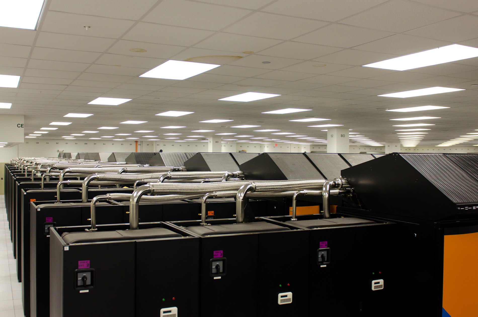
Oak Ridge National Laboratory's Titan Supercomputer
Or perhaps as it’s better known, the GPU at the heart of the world’s fastest supercomputer, Oak Ridge National Laboratory’s Titan supercomputer.
The Titan supercomputer was a major win for NVIDIA, and likely the breakthrough they’ve been looking for. A fledging business merely two generations prior, NVIDIA and their Tesla family have quickly shot up in prestige and size, much to the delight of NVIDIA. Their GPU computing business is still relatively small – consumer GPUs dwarf it and will continue to do so for the foreseeable future – but it’s now a proven business for NVIDIA. More to the point however, winning contracts like Titan are a major source of press and goodwill for the company, and goodwill the company intends to capitalize on.
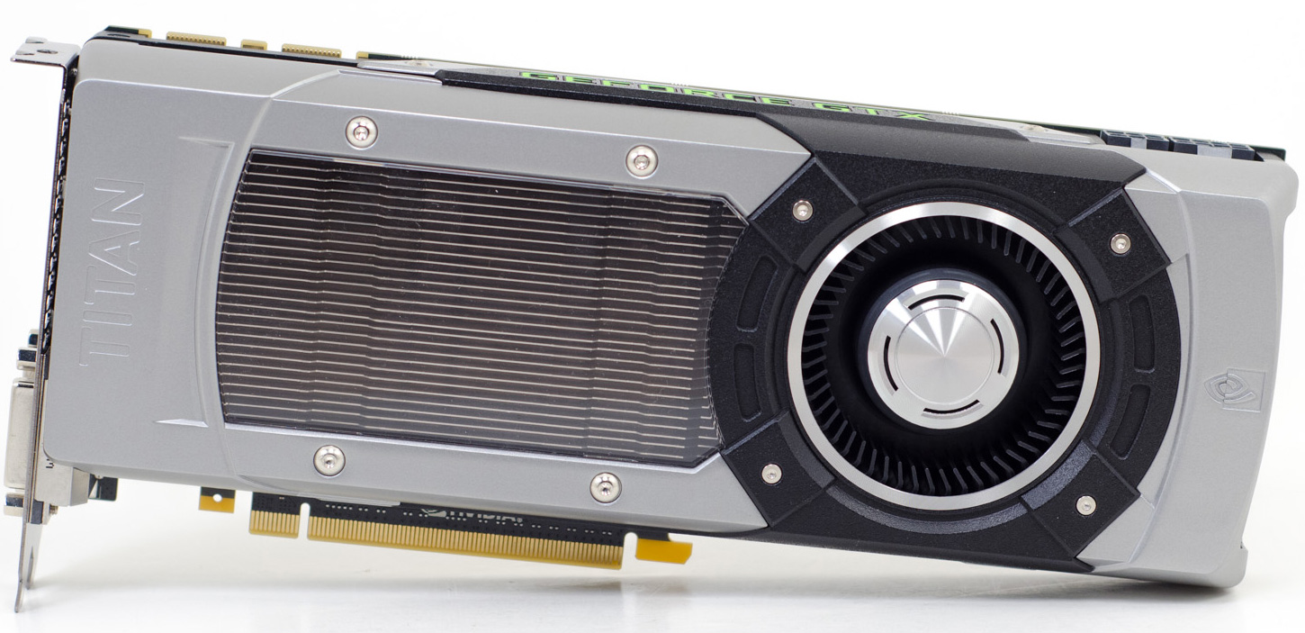
With the launch of the Titan supercomputer and the Tesla K20 family now behind them, NVIDIA is now ready to focus their attention back on the consumer market. Ready to bring their big and powerful GK110 GPU to the consumer market, in typical NVIDIA fashion they intend to make a spectacle of it. In NVIDIA’s mind there’s only one name suitable for the first consumer card born of the same GPU as their greatest computing project: GeForce GTX Titan.
GeForce GTX Titan: By The Numbers
At the time of the GK110 launch at GTC, we didn’t know if and when GK110 would ever make it down to consumer hands. From a practical perspective GTX 680 was still clearly in the lead over AMD’s Radeon HD 7970. Meanwhile the Titan supercomputer was a major contract for NVIDIA, and something they needed to prioritize. 18,688 551mm2 GPUs for a single customer is a very large order, and at the same time orders for Tesla K20 cards were continuing to pour in each and every day after GTC. In the end, yes, GK110 would come to the consumer market. But not until months later, after NVIDIA had the chance to start filling Tesla orders. And today is that day.
Much like the launch of the GTX 690 before it, NVIDIA intends to stretch this launch out a bit to maximize the amount of press they get. Today we can tell you all about Titan – its specs, its construction, and its features – but not about its measured performance. For that you will have to come back on Thursday, when we can give you our benchmarks and performance analysis.
| GTX Titan | GTX 690 | GTX 680 | GTX 580 | |
| Stream Processors | 2688 | 2 x 1536 | 1536 | 512 |
| Texture Units | 224 | 2 x 128 | 128 | 64 |
| ROPs | 48 | 2 x 32 | 32 | 48 |
| Core Clock | 837MHz | 915MHz | 1006MHz | 772MHz |
| Shader Clock | N/A | N/A | N/A | 1544MHz |
| Boost Clock | 876Mhz | 1019MHz | 1058MHz | N/A |
| Memory Clock | 6.008GHz GDDR5 | 6.008GHz GDDR5 | 6.008GHz GDDR5 | 4.008GHz GDDR5 |
| Memory Bus Width | 384-bit | 2 x 256-bit | 256-bit | 384-bit |
| VRAM | 6 | 2 x 2GB | 2GB | 1.5GB |
| FP64 | 1/3 FP32 | 1/24 FP32 | 1/24 FP32 | 1/8 FP32 |
| TDP | 250W | 300W | 195W | 244W |
| Transistor Count | 7.1B | 2 x 3.5B | 3.5B | 3B |
| Manufacturing Process | TSMC 28nm | TSMC 28nm | TSMC 28nm | TSMC 40nm |
| Launch Price | $999 | $999 | $499 | $499 |
Diving right into things then, at the heart of the GeForce GTX Titan we have the GK110 GPU. By virtue of this being the 2nd product to be launched based off the GK110 GPU, there are no great mysteries here about GK110’s capabilities. We’ve covered GK110 in depth from a compute perspective, so many of these numbers should be familiar with our long-time readers.
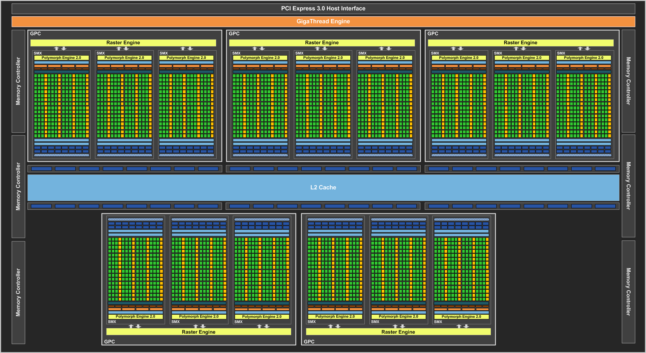
GK110 is composed of 15 of NVIDIA’s SMXes, each of which in turn is composed of a number of functional units. Every GK110 packs 192 FP32 CUDA cores, 64 FP64 CUDA cores, 64KB of L1 cache, 65K 32bit registers, and 16 texture units. These SMXes are in turn paired with GK110’s 6 ROP partitions, each one composed of 8 ROPs, 256KB of L2 cache, and connected to a 64bit memory controller. Altogether GK110 is a massive chip, coming in at 7.1 billion transistors, occupying 551mm2 on TSMC’s 28nm process.
For Titan NVIDIA will be using a partially disabled GK110 GPU. Titan will have all 6 ROP partitions and the full 384bit memory bus enabled, but only 14 of the 15 SMXes will be enabled. In terms of functional units this gives Titan a final count of 2688 FP 32 CUDA cores, 896 FP64 CUDA cores, 224 texture units, and 48 ROPs. This makes Titan virtually identical to NVIDIA’s most powerful Tesla, K20X, which ships with the same configuration. NVIDIA does not currently ship any products with all 15 SMXes enabled, and though NVIDIA will never really explain why this is – yield, power, or otherwise – if nothing else it leaves them an obvious outlet for growth if they need to further improve Titan’s performance, by enabling that 15th SMX.
Of course functional units are only half the story, so let’s talk about clockspeeds. As a rule of thumb bigger GPUs don’t clock as high as smaller GPUs, and Titan will be adhering to this rule. Whereas GTX 680 shipped with a base clock of 1006MHz, Titan ships at a more modest 837MHz, making up for any clockspeed disadvantage with the brute force behind having so many functional units. Like GTX 680 (and unlike Tesla), boost clocks are once more present, with Titan’s official boost clock coming in at 876MHz, while the maximum boost clock can potentially be much higher.
On the memory side of things, Titan ships with a full 6GB of GDDR5. As a luxury card NVIDIA went for broke here and simply equipped the card with as much RAM as is technically possible, rather than stopping at 3GB. You wouldn’t know that from looking at their memory clocks though; even with 24 GDDR5 memory chips, NVIDIA is shipping Titan at the same 6GHz effective memory clock as the rest of the high-end GeForce 600 series cards, giving the card 288GB/sec of memory bandwidth.
To put all of this in perspective, on paper (and at base clocks), GTX 680 can offer just shy of 3.1 TFLOPS of FP32 performance, 128GTexels/second texturing throughput, and 32GPixels/second rendering throughput, driven by 192GB/sec of memory bandwidth. Titan on the other hand can offer 4.5 TFLOPS of FP32 performance, 187GTexels/second texturing throughput, 40GPixels/second rendering throughput, and is driven by a 288GB/sec memory bus. This gives Titan 46% more shading/compute and texturing performance, 25% more pixel throughput, and a full 50% more memory bandwidth than GTX 680. Simply put, thanks to GK110 Titan is a far more powerful GPU than what GK104 could accomplish.
Of course with great power comes great power bills, to which Titan is no exception. In GTX 680’s drive for efficiency NVIDIA got GTX 680 down to a TDP of 195W with a power target of 170W, a remarkable position given both the competition and NVIDIA’s prior generation products. Titan on the other hand will have a flat 250W power target – in line with prior generation big NVIDIA GPUs – staking out its own spot on the price/power hierarchy, some 28%-47% higher in power consumption than GTX 680. These values are almost identical to the upper and lower theoretical performance gaps between Titan and GTX 680, so performance is growing in-line with power consumption, but only just. From a practical perspective Titan achieves a similar level of efficiency as GTX 680, but as a full compute chip it’s unquestionably not as lean. There’s a lot of compute baggage present that GK104 didn’t have to deal with.


157 Comments
View All Comments
WhoppingWallaby - Thursday, February 21, 2013 - link
Dude, you have some gall calling another person a fanboy. We could all do without your ranting and raving, so go troll elsewhere or calm down a little.CeriseCogburn - Sunday, February 24, 2013 - link
Oh shut up yourself you radeon rager.You idiots think you have exclusive rights to spew your crap all over the place, and when ANYONE disagrees you have a ***** fit and demand they stop.
How about all you whining critical diaper pooping fanatics stop instead ?
IanCutress - Tuesday, February 19, 2013 - link
It's all about single card performance. Everything just works eaier with a single card. Start putting SLI into the mix and you need to take into account for drivers, or when doing compute it requires a complete reworking of code. Not to mention the potentially lower power output and OC capabilities of Titan over a dual GPU card.At any given price point, getting two cards up to that cost will always be quicker than a single card in any scenario that can take advantage, if you're willing to put up with it. So yes, two GTX 680s, a 690, or a Titan is a valid question, and it's up to the user preference which one to get.
I need to double check my wallet, see if it hasn't imploded after hearing the price.
wreckeysroll - Tuesday, February 19, 2013 - link
lost their minds?how about fell and cracked their head after losing it. Smoking too much of that good stuff down there in California.
How stupid do they take us for. Way to thumb your customers in the eye nvidia. $1000 on a single gpu kit.
Good laugh for the morning.
B3an - Tuesday, February 19, 2013 - link
Use some ****ing common sense. You get what you pay for.6GB with 386-bit memory bus, and a 551mm2 size GPU. Obviously this wont be cheap and theres no way this could be sold for anywhere near the price of a 680 without losing tons of money.
Nvidia already had this thing in super computers anyway so why not turn it in to a consumer product? Some people WILL buy this. If you have the money why not. Atleast NV are not sitting on their arses like AMD are with no new high-end GPU's this year. Even though i have AMD cards i'm very disappointed with AMD's crap lately as an enthusiast and someone who's just interested in GPU tech. First they literally give up on competitive performance CPU's and now it's looking like they're doing it with GPU's.
siliconfiber - Tuesday, February 19, 2013 - link
Common sense is what you are missing.GTX 580, 480, 285 were all sold to for much less than this card and were all used in HPC applications, had the same or much bigger dies sizes, and the same or bigger bus. DDR memory is dirt cheap as well
I have seen it all now. Largest rip-off in the history of video cards right here.
Genx87 - Tuesday, February 19, 2013 - link
Oh look I have never seen this argument before. Biggest rip off in history of video cards. Pre-ceded only by every high end video card release since the introduction of high end discrete GPUs. And will remain a ripoff until the next high end GPU is released surpassing this card ripoff factor.Blibbax - Tuesday, February 19, 2013 - link
It's not a rip off because you don't have to buy it. The 680 hasn't gotten any slower.Just like with cars and anything else, when you add 50% more performance to a high-end product, it's gunna be a lot more than 50% more expensive.
johnthacker - Tuesday, February 19, 2013 - link
The largest rip-off in the history of video cards are some of the Quadro cards. This is extremely cheap for a card with so good FP64 performance.TheJian - Wednesday, February 20, 2013 - link
GTX580 (40nm) was not in the same league as this and only had 3b transistors. Titan has 7.1B on 28nm. 512cuda cores compared to 2880? It came with 1.5GB memory too, this has 6. etc etc..The 580 did not run like a $2500 pro card @ a 1500 discount either. Also a chip this complicated doesn't YIELD well. It's very expensive to toss out the bad ones.Do you know the difference between system memory and graphics memory (you said ddr). They do not cost the same. You meant GDDR? Well this stuff is 4x as much running 6ghz not 4ghz.
Ref clock is 876 but these guys got theirs to 1176:
http://www.guru3d.com/articles-pages/geforce_gtx_t...
The card is a monster value vs. $2500 K20. Engineering is not FREE. Ask AMD. They lost 1.18B last year selling crap at prices that would make you happy I guess. That's how you go out of business. Get it? They haven't made money in 10yrs (lost 3-4B over that time as a whole). Think they should've charged more for their cards/chips the last ten years? I DO. If Titan is priced wrong, they will remain on the shelf. Correct? So if you're right they won't sell. These will be gone in a day, because there are probably enough people that would pay $1500 for them they'll sell out quickly. You have to pay $2500 to get this on the pro side.