Crossbar's Resistive RAM Technology Reaching Commercialisation Stage
by Kristian Vättö on December 21, 2014 4:35 PM EST- Posted in
- Storage
- SSDs
- Resistive RAM
- RRAM
- Crossbar

While the first 3D NAND chips have just found their way to the market and most NAND manufacturers are still developing their designs, there are already a handful of next generation memory technologies in development that are slated to supersede NAND in the next decade or so. One of the most promising technologies is Resistive Random Access Memory, which is more commonly referred to as Resistive RAM or just RRAM. Similar to NAND, RRAM is non-volatile, meaning that it will retain data without power unlike regular DRAM, which needs a continuous power source. Multiple companies are developing RRAM including semiconductor giants like Samsung and SanDisk, but Crossbar, a US based startup, has probably the most advanced design so far.
I've been following Crossbar for quite some time, but I haven't written anything about the company until now. The company was founded in 2010, headquarters in Santa Clara, California and has secured over $50 million in funding. The company's roots come from the University of Michigan and its Chief Scientist and co-founder, Prof. Wei Lu, is currently an associate professor at the university. The Crossbar team consists of 40-45 members at this point, of which most have extensive backgrounds in semiconductor research and development.
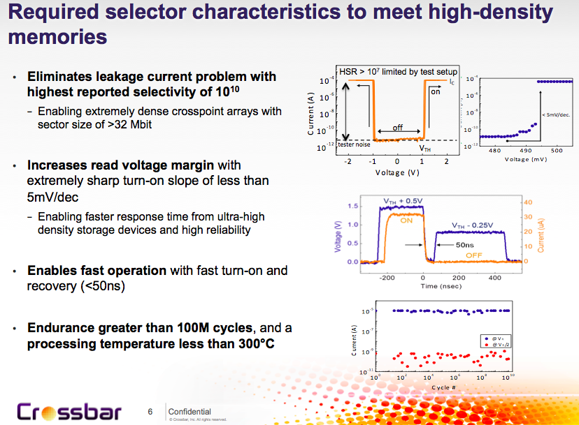
The big benefits RRAM have over NAND are performance and endurance. NAND read latencies are typically in the order of hundreds of microseconds, whereas Crossbar claims latency of as low as 50 nanoseconds for its RRAM design. Endurance in turn can be millions of program/erase cycles, although for the early designs Crossbar is aiming at more conservative ~100K cycles.
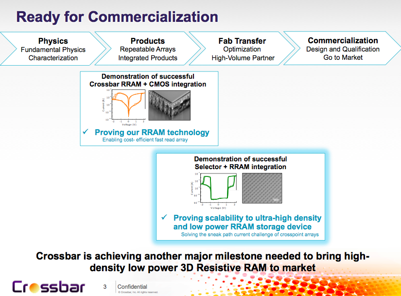
Last week at IEDM Crossbar announced that it is now entering the commercialization stage. In other words, it has already shown a working silicon and it has also proved that the design can be transferred to commercial fab for high volume manufacturing, so the company is now working with the fabs to build final products.
At first Crossbar is aiming at the embedded market and is licensing its technology to ASIC, FPGA and SoC developers with first samples arriving in early 2015, and mass production scheduled for late 2015 or early 2016. Aside from licensing, Crossbar is also developing standalone chips with higher capacity and density, which should enter the market about a year after the embedded RRAM designs (i.e.most likely sometime in 2017).
The beauty of RRAM is that it can be manufactured using a regular CMOS process with only a few modifications. NAND and especially 3D NAND require expensive special tools (for things like high aspect ratio etching), which is why only a handful of companies are making 3D NAND. RRAM in turn can be manufactured by practically any existing fab with very little added cost, which ultimately results in lower prices due to more competition.
Additionally, RRAM doesn't share NAND's lithography issues. As we know, the sole reason why 3D NAND was invented is because planar NAND can't really scale below 15nm without serious endurance and performance considerations. However, RRAM can efficiently scale to 4-5nm without any issues and in fact Crossbar has already demonstrated an 8nm chip that it built in its R&D labs (most likely using multiple patterning). Moreover, RRAM can be stacked vertically to create a 3D crosspoint array for increased density and so far Crossbar is at three layers, but first commercial standalone chips are expected to feature 16 layers and up to 1Tbit capacity.
Obviously, there are still several hurdles to cross before RRAM is ready to challenge NAND, but it's good to hear that there has been significant progress in development and the technology has gained interest from the fab companies. Faster, more durable and cheaper SSDs and other storage devices are a win for everyone and ultimately even 3D NAND is just an interim solution until something better comes around, which may very well be RRAM. I'll be doing a more in-depth article about RRAM technology in the coming months as this article was more of a heads up about the state of RRAM and Crosspoint's recent developments, so stay tuned for a deeper analysis!


65 Comments
View All Comments
metayoshi - Tuesday, December 23, 2014 - link
You wouldn't need TRIM anymore since Kristian said that blocks can be overwritten in a previous comment. The reason TRIM was needed on an SSD was because once you write to a NAND block, it would need to be erased before writing to it again, and the erasing caused a huge performance degradation to future writes. TRIM tells the NAND controller that these specific blocks are not being used by the OS or firmware anymore, so that it can preemptively erase the block in the background (or during the TRIM command) in order for future writes to that block to be as fast as the first write. For RRAM, if overwriting a block has no performance penalty compared to writing data from a "clean" block, like in HDDs, TRIM has no benefit at all.JonnyDough - Wednesday, December 24, 2014 - link
HDD's lose capacity over time as well, they just mark sectors as bad if they can't repair it. SSD trim functionality does the same doesn't it? What happens if a block goes bad? What happens if an entire chip dies to overvoltage or something? Why should you lose all your data? Isn't parity built into the drive? If each chip isn't being "RAID 5'd" then it should be for consumer drives at the 1TB level I think.JonnyDough - Wednesday, December 24, 2014 - link
You'd still utilize it simply to maintain fuller capacity. Regardless of overall life expectancy, parts of the drive will undoubtedly go bad with use, as with current NAND technology. Wear leveling will help to minimize these failures. Just because it may happen much much less frequently does not mean it won't happen some - although the more resolute the storage medium the less important wear leveling becomes.JonnyDough - Wednesday, December 24, 2014 - link
Apple will adopt it. Elitists don't care about cost. LOL Once Apple buys in and it lowers the cost due to economies of scale everyone else will follow suit. The first to successfully fab this is going to make a LOT of money - I just wish I could tell who it was going to be so I could sell everything I own and invest at the right moment.p1esk - Tuesday, December 23, 2014 - link
DDR memory access time is about 100ns, not 10ns.rkcth - Sunday, December 21, 2014 - link
50 ns as in 1/000 of a microsecond. It's still several times slower than typical RAM I think, but MUCH faster than NAND (by about 100X).Jaybus - Saturday, January 3, 2015 - link
The 50 ns is the switching time, or the time it takes to switch a cell from a 0 to a 1 or a 1 to a 0. Actual write time is going to be longer due to addressing overhead, just as with DRAM. It will still be at least 20x faster than NAND, so a significant performance advantage. The biggest advantage, of course, is that it requires only a tiny 4F cell size and is expected to function at sub-10 nm, meaning it will be much more dense than NAND. Another advantage is that it can operate at lower voltage than NAND, so should use less power.CaedenV - Sunday, December 21, 2014 - link
Very interesting. Hyper Memory Cube tech is supposed to act as a RAM+Flash replacement, but is super expensive. Would RRAM be fast enough to use as both internal memory and storage? Or would this stick to the more traditional model of still needing DRAM for active memory? 50ns may be slow for a desktop PC, but for a phone or tablet it would not be all that bad, plus just having to flag memory between storage and active RAM would dramatically reduce load times. Not to mention one less part is one less part... I would much rather have something cheap like RRAM than something expensive like HMC.menting - Monday, December 22, 2014 - link
HMC isn't targeted as a RAM+FLASH replacement. It's targeted at high performance memory in a limited space, as well as less energy used per bit, which RRAM is defintely not targeted for in the short term.p1esk - Tuesday, December 23, 2014 - link
50ns is not slow for a traditional PC. DDR memory access time is about 100ns.