NVIDIA Tegra X1 Preview & Architecture Analysis
by Joshua Ho & Ryan Smith on January 5, 2015 1:00 AM EST- Posted in
- SoCs
- Arm
- Project Denver
- Mobile
- 20nm
- GPUs
- Tablets
- NVIDIA
- Cortex A57
- Tegra X1
Tegra X1's GPU: Maxwell for Mobile
Going into today’s announcement of the Tegra X1, while NVIDIA’s choice of CPU had been something of a wildcard, the GPU was a known variable. As announced back at GTC 2014, Erista – which we now know as Tegra X1 – would be a future Tegra product with a Maxwell GPU.
Maxwell of course already launched on the PC desktop as a discrete GPU last year in the Maxwell 1 based GM107 and Maxwell 2 based GM204. However despite this otherwise typical GPU launch sequence, Maxwell marks a significant shift in GPU development for NVIDIA that is only now coming to completion with the launch of the X1. Starting with Maxwell, NVIDIA has embarked on a “mobile first” design strategy for their GPUs; unlike Tegra K1 and its Kepler GPU, Maxwell was designed for Tegra from the start rather than being ported after the fact.
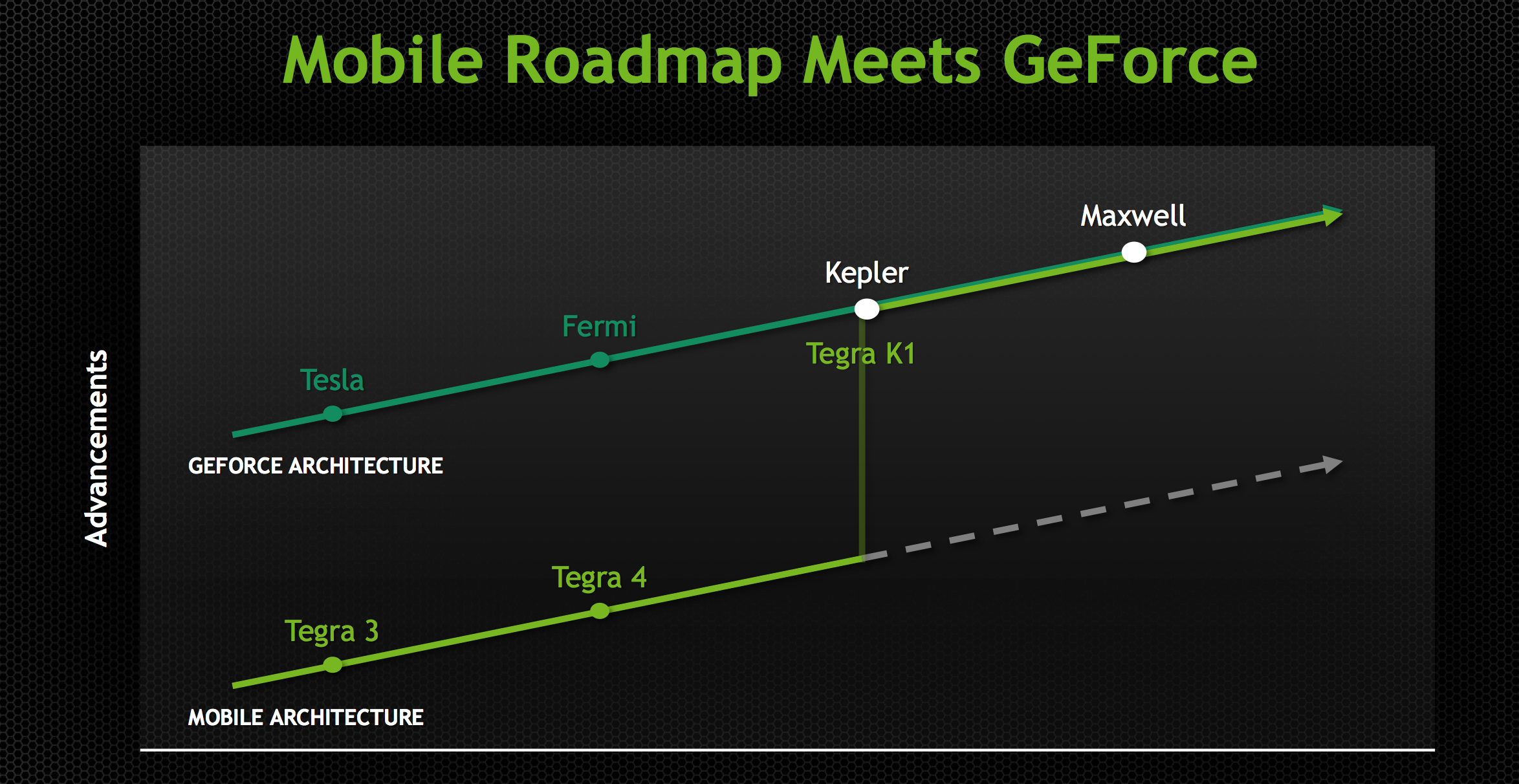
By going mobile-first NVIDIA has been able to reap a few benefits. On the Tegra side in particular, mobile-first means that NVIDIA’s latest and greatest GPUs are appearing in SoCs earlier than ever before – the gap between Maxwell 1 and Tegra X1 is only roughly a year, versus nearly two years for Kepler in Tegra K1. But it also means that NVIDIA is integrating deep power optimizations into their GPU architectures at an earlier stage, which for their desktop GPUs has resulted chart-topping power efficiency, and these benefits are meant to cascade down to Tegra as well.
Tegra X1 then is the first SoC to be developed under this new strategy, and for NVIDIA this is a very big deal. From a feature standpoint NVIDIA gets to further build on their already impressive K1 feature set with some of Maxwell’s new features, and meanwhile from a power standpoint NVIDIA wants to build the best A57 SoC on the market. With everyone else implementing (roughly) the same CPU, the GPU stands to be a differentiator and this is where NVIDIA believes their GPU expertise translates into a significant advantage.
Diving into the X1’s GPU then, what we have is a Tegra-focused version of Maxwell 2. Compared to Kepler before it, Maxwell 2 introduced a slew of new features into the NVIDIA GPU architecture, including 3rd generation delta color compression, streamlined SMMs with greater efficiency per CUDA core, and graphics features such as conservative rasterization, volumetric tiled resources, and multi-frame anti-aliasing. All of these features are making their way into Tegra X1, and for brevity’s sake rather than rehashing all of this we’ll defer to our deep dive on the Maxwell 2 architecture from the launch of the GeForce GTX 980.
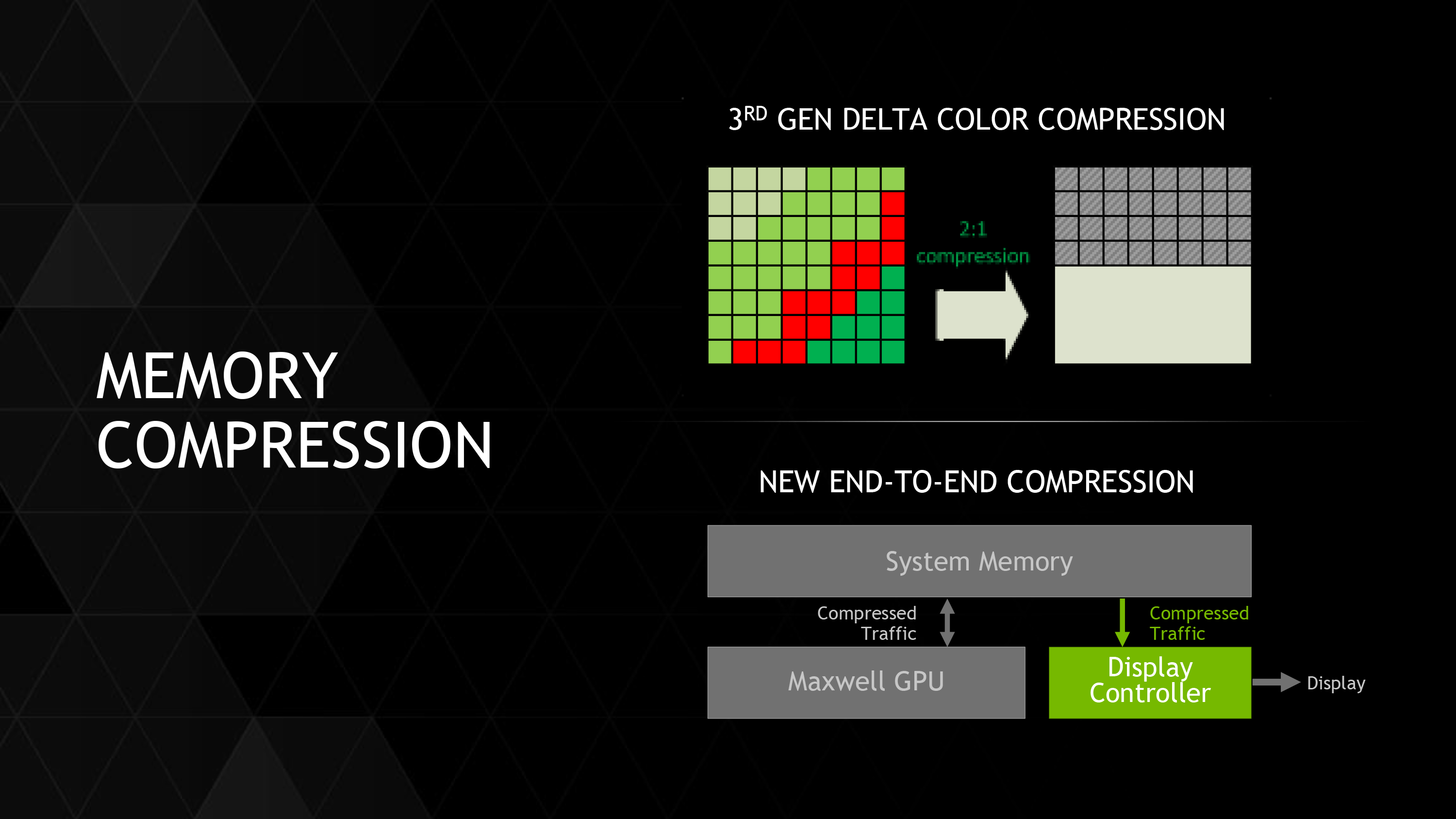
For X1 in particular, while every element helps, NVIDIA’s memory bandwidth and overall efficiency increases are going to be among the most important of these improvements since they address two of the biggest performance bottlenecks facing SoC-class GPUs. In the case of memory bandwidth optimizations, memory bandwidth has long been a bottleneck at higher performance levels and resolutions, and while it’s a solvable problem, the general solution is to build a wider (96-bit or 128-bit) memory bus, which is very effective but also drives up the cost and complexity of the SoC and the supporting hardware. In this case NVIDIA is sticking to a 64-bit memory bus, so memory compression is very important for NVIDIA to help drive X1. This coupled with a generous increase in memory bandwidth from the move to LPDDR4 helps to ensure that X1’s more powerful GPU won’t immediately get starved at the memory stage.
Meanwhile just about everything about SoC TDP that can be said has been said. TDP is a limiting factor in all modern mobile devices, which means deceased power consumption directly translates into increased performance, especially under sustained loads. Coupled with TSMC’s 20nm SoC process, Maxwell’s power optimizations will further improve NVIDIA’s SoC GPU performance.
Double Speed FP16
Last but certainly not least however, X1 will also be launching with a new mobile-centric GPU feature not found on desktop Maxwell. For X1 NVIDIA is implanting what they call “double speed FP16” support in their CUDA cores, which is to say that they are implementing support for higher performance FP16 operations in limited circumstances.
As with Kepler and Fermi before it, Maxwell only features dedicated FP32 and FP64 CUDA cores, and this is still the same for X1. However in recognition of how important FP16 performance is, NVIDIA is changing how they are handling FP16 operations for X1. On K1 FP16 operations were simply promoted to FP32 operations and run on the FP32 CUDA cores; but for X1, FP16 operations can in certain cases be packed together as a single Vec2 and issued over a single FP32 CUDA core.
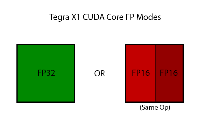
There are several special cases here, but in a nutshell NVIDIA can pack together FP16 operations as long as they’re the same operation, e.g. both FP16s are undergoing addition, multiplication, etc. Fused multiply-add (FMA/MADD) is also a supported operation here, which is important for how frequently it is used and is necessary to extract the maximum throughput out of the CUDA cores.
In this respect NVIDIA is playing a bit of catch up to the competition, and overall it’s hard to escape the fact that this solution is a bit hack-ish, but credit where credit is due to NVIDIA for at least recognizing and responding to what their competition has been doing. Both ARM and Imagination have FP16 capabilities on their current generation parts (be it dedicated FP16 units or better ALU decomposition), and even AMD is going this route for GCN 1.2. So even if it only works for a few types of operations, this should help ensure NVIDIA doesn’t run past the competition on FP32 only to fall behind on FP16.
So why are FP16 operations so important? The short answer is for a few reasons. FP16 operations are heavily used in Android’s display compositor due to the simplistic (low-precision) nature of the work and the power savings, and FP16 operations are also used in mobile games at certain points. More critical to NVIDIA’s goals however, FP16 can also be leveraged for computer vision applications such as image recognition, which NVIDIA needs for their DRIVE PX platform (more on that later). In both of these cases FP16 does present its own limitations – 16-bits just isn’t very many bits to hold a floating point number – but there are enough cases where it’s still precise enough that it’s worth the time and effort to build in the ability to process it quickly.
Tegra X1 GPU By The Numbers
Now that we’ve covered the X1’s GPU from a feature perspective, let’s take a look the GPU from a functional unit/specification perspective.
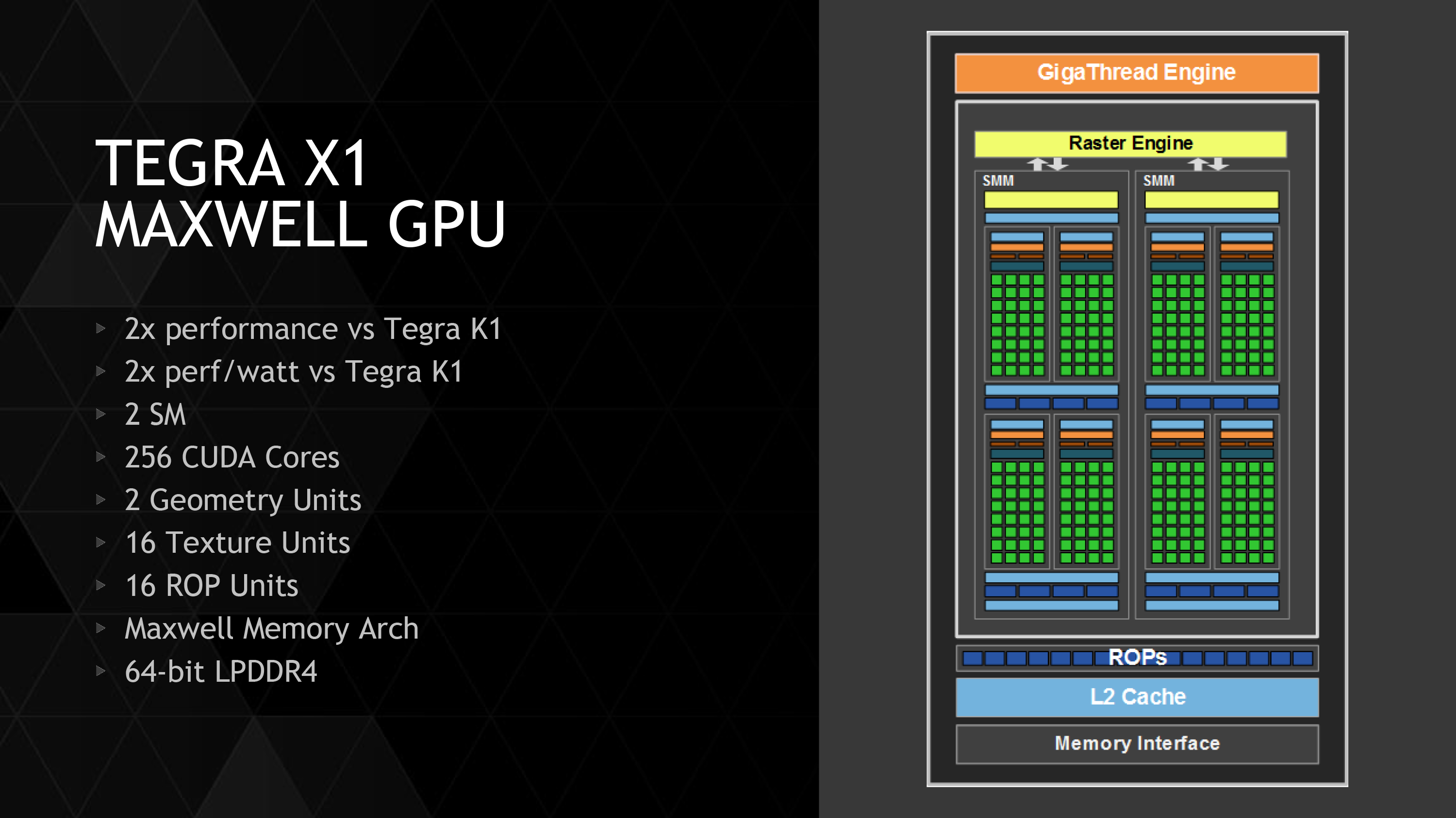
Overall the X1’s GPU is composed of 2 Maxwell SMMs inside a single GPC, for a total of 256 CUDA cores. This compares very favorably to the single SMX in K1, as it means certain per-SMM/SMX resources such as the geometry and texture units have been doubled. Furthermore Maxwell’s more efficient CUDA cores means that X1 is capable of further extending its lead over Kepler, as we’ve already seen in the desktop space.
| NVIDIA Tegra GPU Specification Comparison | ||||
| K1 | X1 | |||
| CUDA Cores | 192 | 256 | ||
| Texture Units | 8 | 16 | ||
| ROPs | 4 | 16 | ||
| GPU Clock | ~950MHz | ~1000MHz | ||
| Memory Clock | 930MHz (LPDDR3) | 1600MHz (LPDDR4) | ||
| Memory Bus Width | 64-bit | 64-bit | ||
| FP16 Peak | 365 GFLOPS | 1024 GFLOPS | ||
| FP32 Peak | 365 GFLOPS | 512 GFLOPS | ||
| Architecture | Kepler | Maxwell | ||
| Manufacturing Process | TSMC 28nm | TSMC 20nm SoC | ||
Meanwhile outside of the CUDA cores NVIDIA has also made an interesting move in X1’s ROP configuration. At 16 ROPs the X1 has four times the ROPs of K1, and is consequently comparatively ROP heavy. This is as many ROPs as is on a GM107 GPU, for example. With that said, due to NVIDIA’s overall performance goals and their desire to drive 4K displays at 60Hz, there is a definite need to go ROP-heavy to make sure they can push the necessary amount of pixels. This also goes hand-in-hand with NVIDIA’s memory bandwidth improvements (efficiency and actual) which will make it much easier to feed those ROPs. This also puts the ROP:memory controller ratio at 16:1, the same ratio as on NVIDIA’s desktop Maxwell parts.
Finally, let’s talk about clockspeeds and expected performance. While NVIDIA is not officially publishing the GPU clockspeeds for the X1, based on their performance figures it’s easy to figure out. With NVIDIA’s quoted (and promoted) 1 TFLOPs FP16 performance figure for the X1, the clockspeed works out to a full 1GHz for the GPU (1GHz * 2 FP 16 * 2 FMA * 256 = 1 TFLOPs).
This is basically a desktop-class clockspeed, and it goes without saying that is a very aggressive GPU clockspeed for an SoC-class part. We’re going to have to see what design wins X1 lands and what the devices are like, but right now it’s reasonable to expect that mobile devices will only burst here for short periods of time at best. However NVIDIA’s fixed platform DRIVE devices are another story; those can conceivably be powered and cooled well enough that the X1’s GPU can hit and sustain these clockspeeds.


194 Comments
View All Comments
Mayuyu - Monday, January 5, 2015 - link
Apple should start licensing Nvidia GPUs instead of Imagination GPUs for next generation iDevices.twotwotwo - Monday, January 5, 2015 - link
It might be hard (or impossible) for them to do that without breaking compatibility with existing iOS games written around the PowerVR's quirks.Krysto - Monday, January 5, 2015 - link
The OpenGL stuff shouldn't be "impossible". Even the texture compression. I think developers can deal with that. Where Apple really shot itself in the foot is with the launch of the Metal API, though. Now they're stuck with Imagination for at least a few more years until they make it more abstract to work with multiple GPU architectures and not so..."metal". Or they can wait for OpenGL NG to appear, which will probably take just as much time.techconc - Monday, January 5, 2015 - link
How exactly did Apple "shoot itself in the foot" with Metal. They have a solution right now for mobile apps that rivals what is possible on other platforms. All the major game engines have already migrated to Metal. nVidia can show these generic OpenGL benchmarks all they want, but in practice, graphic intensive apps on the A7 and A8 series chips are seeing far greater efficiency and performance improvements.OpenGL NG sounds great in concept, but it takes forever for a consortium like Khronos to develop new standards and just as long for them to eventually be adopted. This is years away from becoming a reality. Yet, Apple gets all of the benefits of that right now. From my perspective, this gives Apple a strong competitive advantage.
akdj - Sunday, January 11, 2015 - link
Well said techconcNot sure if you're in to development, SoC design or just a 'user', Krysto...but BOTH Apple's 'Metal' and language 'Swift' were/are HUGE leaps forward to 'cut' the peanut butter layer on the GPU that is Open GL ES ...so developers have 'direct' access to the 'metal' AKA GPU portion of the SoC. It's an amazing feat in 'software engineering' that helped a huge load on the 'hardware engineering' side of the house....specifically because of this!
I own a Note 4 for my business
I own a 6+ as a personal driver.
The former a quad core, 2.7x Ghz procs and the Adreno 420 and 3GB of 'shared' SoC RAM
The latter, a dual core, 1.5Ghz procs with IT's solution for graphics and 1GB of 'shared' SoC RAM
I love them both, different reasons BUT, Play Asphalt 8 on both. Then tell me 'more muscle, power, RAM, cores or core speed' are the reasons I'm playing a more fluent game on iOS vs android
I'm ambidextrous and enjoy using both. Same in the office or home environment. OS X is primary but I've always had a Windows box since the big 'switch' a decade ago
Point being, software is damn near, and sometimes MORE important than hardware to the end user's experience. No one outside of us dorks, geeks, and pocket protector wearing Homers has a clue what FitFat, latency, core clock speed, or hell....cores for that matter MEAN! They couldn't tell Ya if theyre rocking 1, 2, 3 GB of RAM or NO RAM, lol.
The ultimate end experience is designed and defined by the software and hardware working in synergy WITH a development community willing to step up and develop a million optomized apps for your system. If it's running iOS or Android, you're in luck. Windows, a bit tougher to 'win' and if this SoC does indeed have the power/TDP numbers they're bragging, Apple's never been one to change supply chains
There's a reason Tim is CEO, & that's the biggest. When you're dropping 100,000 products a year, you HAVE to have suppliers that can fulfill your orders and needs
adriaaaaan - Thursday, January 15, 2015 - link
Are you honestly expecting a phone with a weaker GPU pushing 50% more pixels to out perform the other? Of course the iPhone is smoother in games its lower res than the note 4Maleficum - Wednesday, January 21, 2015 - link
Oh yeah, Note4 has to push more pixels than 6+. However, a resolution that high is simply not necessary in first place, and more importantly, over 30% of the pixel data the SoC has to process are nullified by the pentiled AMOLED. What a waste!Maxjonny55 - Saturday, June 20, 2015 - link
Metal has made easier for to access the GPU and the reason apple had done this due the lack of power on there CPUs compared to android device, yes sure GPUs can run apps with extra power but then so what? Open GL has always been doing that! More will know Java and Open GL and easier for development as all hardware vendor apart from apple will optimise hardware for it.I would not want to compare Asphalt 8 between devices as horse power and muscle has nothing to do with it but lazy work on the part of game creators.
Providing access to metal will make a difference to apps no doubt but some apps and not all.. Open GL provides access to GPU not sure why it took apple so long. I have a Nexus 9 and iPad Air 2 and can't see apart from Apple hype what the Air 2 had to offer in performance! Nexus 9 single core out performes the Air 2 and so does the 1 year older GPU..
Wolfpup - Wednesday, September 30, 2015 - link
"lack of power"? Apple's CPUs blow away any other ARM CPUs.Maleficum - Wednesday, January 21, 2015 - link
OpenGL is FAR outdated. It has way too many performance bottlenecks due to the aged design, and doesn't scale very well with modern GPU/CPU architectures.Both MS and Apple recognized this, et voila, Metal and the upcoming DX12 are their answers.
Pity that Android can't keep up with this, stuck with the opensource mess.