HiSilicon Kirin 960: A Closer Look at Performance and Power
by Matt Humrick on March 14, 2017 7:00 AM EST- Posted in
- Smartphones
- Mobile
- SoCs
- HiSilicon
- Cortex A73
- Kirin 960
GPU Power Consumption and Thermal Stability
GPU Power Consumption
The Kirin 960 adopts ARM’s latest Mali-G71 GPU, and unlike previous Kirin SoCs that tried to balance performance and power consumption by using fewer GPU cores, the 960’s 8 cores show a clear focus on increasing peak performance. More cores also means more power and raises concerns about sustained performance.
We measure GPU power consumption using a method that’s similar to what we use for the CPU. Running the GFXBench Manhattan 3.1 and T-Rex performance tests offscreen, we calculate the system load power by subtracting the device’s idle power from its total active power while running each test, using each device’s onboard fuel gauge to collect data.
| GFXBench Manhattan 3.1 Offscreen Power Efficiency (System Load Power) |
||||
| Mfc. Process | FPS | Avg. Power (W) |
Perf/W Efficiency |
|
| LeEco Le Pro3 (Snapdragon 821) | 14LPP | 33.04 | 4.18 | 7.90 fps/W |
| Galaxy S7 (Snapdragon 820) | 14LPP | 30.98 | 3.98 | 7.78 fps/W |
| Xiaomi Redmi Note 3 (Snapdragon 650) |
28HPm | 9.93 | 2.17 | 4.58 fps/W |
| Meizu PRO 6 (Helio X25) | 20Soc | 9.42 | 2.19 | 4.30 fps/W |
| Meizu PRO 5 (Exynos 7420) | 14LPE | 14.45 | 3.47 | 4.16 fps/W |
| Nexus 6P (Snapdragon 810 v2.1) | 20Soc | 21.94 | 5.44 | 4.03 fps/W |
| Huawei Mate 8 (Kirin 950) | 16FF+ | 10.37 | 2.75 | 3.77 fps/W |
| Huawei Mate 9 (Kirin 960) | 16FFC | 32.49 | 8.63 | 3.77 fps/W |
| Galaxy S6 (Exynos 7420) | 14LPE | 16.62 | 4.63 | 3.59 fps/W |
| Huawei P9 (Kirin 955) | 16FF+ | 10.59 | 2.98 | 3.55 fps/W |
The Mate 9’s 8.63W average is easily the highest of the group and simply unacceptable for an SoC targeted at smartphones. With the GPU consuming so much power, it’s basically impossible for the GPU and even a single A73 CPU core to run at their highest operating points at the same time without exceeding a 10W TDP, a value more suitable for a large tablet. The Mate 9 allows its GPU to hit 1037MHz too, which is a little silly. For comparison, the Exynos 7420 on Samsung’s 14LPE FinFET process, which also has an 8 core Mali GPU (albeit an older Mali-T760), only goes up to 772MHz, keeping its average power below 5W.
The Mate 9’s average power is 3.1x higher than the Mate 8’s, but because peak performance goes up by the same amount, efficiency turns out to be equal. Qualcomm’s Adreno 530 GPU in Snapdragon 820/821 is easily the most efficient with this workload, and despite achieving about the same performance of Kirin 960, it uses less than half the power.
| GFXBench T-Rex Offscreen Power Efficiency (System Load Power) |
||||
| Mfc. Process | FPS | Avg. Power (W) |
Perf/W Efficiency |
|
| LeEco Le Pro3 (Snapdragon 821) | 14LPP | 94.97 | 3.91 | 24.26 fps/W |
| Galaxy S7 (Snapdragon 820) | 14LPP | 90.59 | 4.18 | 21.67 fps/W |
| Galaxy S7 (Exynos 8890) | 14LPP | 87.00 | 4.70 | 18.51 fps/W |
| Xiaomi Mi5 Pro (Snapdragon 820) | 14LPP | 91.00 | 5.03 | 18.20 fps/W |
| Apple iPhone 6s Plus (A9) [OpenGL] | 16FF+ | 79.40 | 4.91 | 16.14 fps/W |
| Xiaomi Redmi Note 3 (Snapdragon 650) |
28HPm | 34.43 | 2.26 | 15.23 fps/W |
| Meizu PRO 5 (Exynos 7420) | 14LPE | 55.67 | 3.83 | 14.54 fps/W |
| Xiaomi Mi Note Pro (Snapdragon 810 v2.1) |
20Soc | 57.60 | 4.40 | 13.11 fps/W |
| Nexus 6P (Snapdragon 810 v2.1) | 20Soc | 58.97 | 4.70 | 12.54 fps/W |
| Galaxy S6 (Exynos 7420) | 14LPE | 58.07 | 4.79 | 12.12 fps/W |
| Huawei Mate 8 (Kirin 950) | 16FF+ | 41.69 | 3.58 | 11.64 fps/W |
| Meizu PRO 6 (Helio X25) | 20Soc | 32.46 | 2.84 | 11.43 fps/W |
| Huawei P9 (Kirin 955) | 16FF+ | 40.42 | 3.68 | 10.98 fps/W |
| Huawei Mate 9 (Kirin 960) | 16FFC | 99.16 | 9.51 | 10.42 fps/W |
Things only get worse for Kirin 960 in T-Rex, where average power increases to 9.51W and GPU efficiency drops to the lowest value of any device we’ve tested. As another comparison point, the Exynos 8890 in Samsung’s Galaxy S7, which uses a wider 12 core Mali-T880 GPU at up to 650MHz, averages 4.7W and is only 12% slower, making it 78% more efficient.
All of the flagship SoCs we’ve tested from Apple, Qualcomm, and Samsung manage to stay below a 5W ceiling in this test, and even then these SoCs are unable to sustain peak performance for very long before throttling back because of heat buildup. Ideally, we like to see phones remain below 4W in this test, and pushing above 5W just does not make any sense.
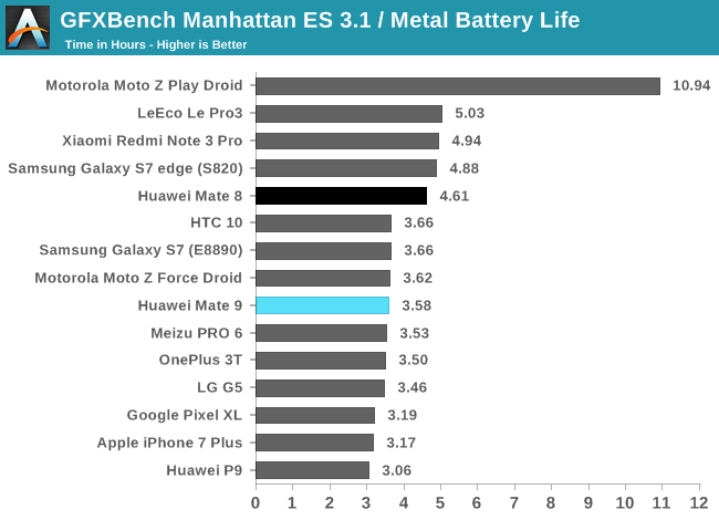
The Kirin 960’s higher power consumption has a negative impact on the Mate 9’s battery life while gaming. It runs for 1 hour less than the Mate 8, a 22% reduction that would be more pronounced it the Mate 9 did not throttle back GPU frequency during the test. Ultimately, the Mate 9’s runtime is similar to other flagship phones (with smaller batteries), while providing similar or better performance. To reconcile Kirin 960’s high GPU power consumption with the Mate 9’s acceptable battery life in our gaming test, we need to look more closely at its behavior over the duration of the test.
GPU Thermal Stability
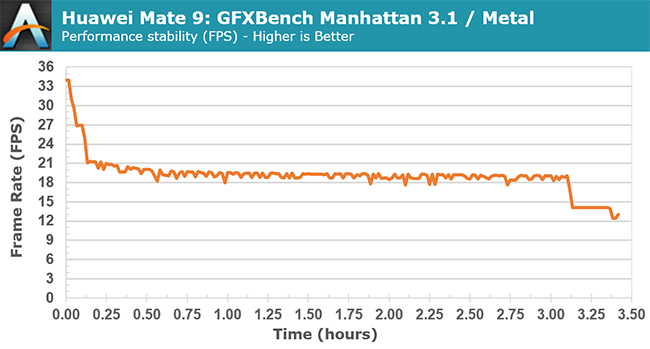
The Mate 9 only maintains peak performance for about 1 minute before reducing GPU frequency, dropping frame rate to 21fps after 8 minutes, a 38% reduction relative to the peak value. It reaches equilibrium after about 30 minutes, with frame rate hovering around 19fps, which is still better than the phones using Kirin 950/955 that peak at 11.5fps with sustained performance hovering between 9-11fps. It’s also as good as or better than phones using Qualcomm’s Snapdragon 820/821 SoCs. The Moto Z Force Droid, for example, can sustain a peak performance of almost 18fps for 12 minutes, gradually reaching a steady-state frame rate of 14.5fps, and the LeEco Pro 3 sustains 19fps after dropping from a peak value of 33fps.
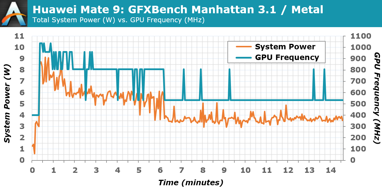
In the lower chart, which shows how the Mate 9’s GPU frequency and power consumption change during the first 15 minutes of the gaming battery test, we can see that once GPU frequency drops to 533MHz, average power consumption drops below 4W, a sustainable value that still results in performance on par with other flagship SoCs after they’ve throttled back too. This suggests that Huawei/HiSilicon should have chosen a more sensible peak operating point for Kirin 960’s GPU of 650MHz to 700MHz. The only reason to push GPU frequency to 1037MHz (at least in a phone or tablet) is to make the device look better on a spec sheet and post higher peak scores in benchmarks.
Lowering GPU frequency would not improve Kirin 960’s low GPU efficiency, however. Because we do not have any other Mali-G71 examples at this time, we cannot say if this is indicative of ARM’s new GPU microarchitecture (I suspect not) or the result of HiSilicon’s implementation and process choice.


86 Comments
View All Comments
BedfordTim - Tuesday, March 14, 2017 - link
I suspect it comes down to cost and usage. The iPhone cores are roughly four times the size of an A73.name99 - Tuesday, March 14, 2017 - link
True. But the iPhone cores are still small ENOUGH. The main CPU complex on an A10 (two big cores, two small cores, and L2, is maybe 15 mm^2.ARM STILL seems to be optimizing for core area, and then spending that same core area anyway in octacores and decacores. It makes no sense to me.
Obviously part of it is that Apple must be throwing a huge number of engineers at the problem. But that's not enough; there has to be some truly incredible project management involved to keep all those different teams in sync, and I don't think anyone has a clue how they have done that.
They certainly don't seem to be suffering from any sort of "mythical man-month" Fred Brooks problems so far...
My personal suspicion is that, by luck or by hiring the best senior engineer in the world, they STARTED OFF at a place that is pretty much optimal for the trajectory they wanted.
They designed a good 3-wide core, then (as far as anyone can tell) converted that to a 6-wide core by clustering and (this is IMPORTANT) not worrying about all the naysayers who said that a very wide core could not be clocked very high.
Once they had the basic 6-wide core in place, they've had a superb platform on top of which different engineers can figure out improved sub-systems and just slot them in when ready. So we had the FP pipeline redesigned for lower latency, we had an extra NEON functional unit added, we've doubtless had constant improvements to branch prediction, I-fetching, pre-fetching, cache placement and replacement; and so on --- but these are all (more or less) "easy" to optimize given a good foundation on which to build.
I suspect, also, that unlike some in the industry, they have been extremely open to new ideas from academia, so that there's an implementation turnaround time of maybe two years or so from encountering a good idea (say a new design for a cluster predictor) through simulating it to validate its value, to implementing it.
I'm guessing that management (again unlike most companies) is willing to entertain a constant stream of ideas (from engineers, from reading the literature, from talking to academics) and to ACCEPT and NOT COMPLAIN about the cost of writing the simulations, in the full understanding that only 5 or 10% of simulated ideas are worth emulating. My guess is that they've managed to increase frequency rapidly (in spite of the 6-wide width) by implementing a constant stream of the various ideas that have been published (and generally mocked or ignored by the industry) for ways to scale things like load-store queues, issue, and rename --- the standard frequency/power pain-points in OoO design.
Meanwhile ARM seems to suffer from terminal effort-wasting. Apple has a great design, which they have been improving every year. ARM's response, meanwhile, has been to hop like a jack rabbit from A57 to A72 to A73, with no obvious conceptual progression. If each design spends time revising basics like the decoder and the optimal pipeline width, there's little time left to perform the huge number of experiments that I think Apple perform to keep honing the branch predictors, the instruction fusion, the pre-fetchers, and so on.
It reminds me of a piece of under-appreciated software, namely Mathematica, which started off with a ridiculously good foundation and horrible performance. But because the foundation was so good, every release had to waste very little time re-inventing the wheel, it could just keep adding and adding, until the result is just unbelievable.
Meteor2 - Wednesday, March 15, 2017 - link
Didn't Jim Keller have something to do with their current architecture?And yes, Apple seems to have excellent project management. Really, they have every stage of every process nailed. They're not the biggest company in the world by accident.
Meteor2 - Wednesday, March 15, 2017 - link
Also don't forget that (like Intel) ARM has multiple design teams. A72 and A73 are from separate teams; from that perspective, ARM's design progression does make sense. The original A73 'deepdive' by Andrei explained it very well.name99 - Wednesday, March 15, 2017 - link
This is a facet of what I said about project management.The issue is not WHY there are separate CPU design teams --- no-one outside the companies cares about the political compromises that landed up at that point.
The issue is --- are separate design teams and restarting each design from scratch a good fit to the modern CPU world?
It seems to me that the answer has been empirically answered as no, and that every company that follows this policy (which seem to include IBM, don't know about QC or the GPU design teams) really ought to rethink. We don't recreate compilers, or browsers, or OS's every few years from scratch, but we seem to have taken it for granted that doing so for CPUs made sense.
I'm not sure this hypothesis explains everything --- no-one outside Apple (and few inside) have the knowledge necessary to answer the question. But I do wonder if the biggest part of Apple's success came from their being a SW company, and thus looking at CPU design as a question of CONSTANTLY IMPROVING a good base, rather than as a question of re-inventing the wheel every few years the way the competition has always done things.
Meteor2 - Wednesday, March 15, 2017 - link
Part of having separate teams is to engender competition; another is to hedge bets and allow risk-taking. Core replacing Netburst is the standard example, I suppose. I'm sure there are others but they aren't coming to mind at the moment... Does replacing Windows CE with Windows 10 count?Meteor2 - Wednesday, March 15, 2017 - link
Methinks it's more to do with Safari having some serious optimisations for browser benchmarks baked in deep.I'd like to see the A10 subjected to GB4 and SpecInt.
name99 - Wednesday, March 15, 2017 - link
The A10 GeekBench numbers are hardly secret. Believe me, they won't make you happy.SPEC numbers, yeah, we're still waiting on those...
name99 - Wednesday, March 15, 2017 - link
Here's an example:https://browser.primatelabs.com/v4/cpu/959859
Summary:
Single-Core Score 3515
Crypto Score 2425
Integer Score 3876
Floating Point Score 3365
Memory Score 3199
The even briefer summary is that basically every sub-benchmark has A10 at 1.5x to 2x the Kirin 960 score. FP is even more brutal with some scores at 3x, and SGEMM at ~4.5x.
(And that's the A10... The A10X will likely be out within a month, likely fabbed on TSMC 10nm, likely an additional ~50% faster...)
Meteor2 - Wednesday, March 15, 2017 - link
Thanks. Would love to see those numbers in Anandtech charts, and normalised for power.