TechInsights Publishes Preliminary Analysis of 3D XPoint Memory
by Billy Tallis on May 27, 2017 8:01 AM EST
Now that the Intel Optane Memory M.2 SSDs are readily available on the open market, anyone with an electron microscope and the skills to use it can begin to probe the secrets of 3D XPoint memory that Intel and Micron have been keeping tightly under wraps since announcing the new technology in August 2015. The reverse engineering experts at TechInsights have been doing just that, and they recently published their initial findings.
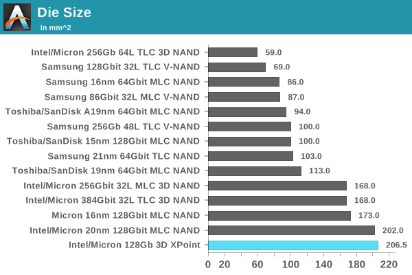
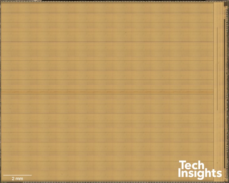
With some of the first high-resolution die photographs of 3D XPoint, TechInsights has provided precise measurements of the die size and memory density. The 128Gb 3D XPoint die is 206.5 mm2, much larger than is typical for modern NAND flash or DRAM but comparable to Intel's 128Gb 20nm planar MLC NAND. A large total die size is typical for Intel and Micron, as they have historically not catered to the mobile market with their NAND flash while competitors like Samsung and Toshiba have strived to ensure their flash will physically fit in devices like smartphones. (That trend is changing with the introduction this year of 64-layer 3D NAND where Intel and Micron are producing both a larger 512Gb TLC part and a smaller 256Gb TLC part.)
The Intel Optane SSD DC P4800X is using memory of similar density to the Intel SSD DC P3700 that it is displacing as the flagship of Intel's SSD product line. When comparing similar chips, die size is a strong predictor of manufacturing cost, but 3D XPoint memory is quite different from NAND flash memory, both older planar NAND or newer 3D NAND. Still, there's some value in noting that the P4800X is arriving with a price tag about 25% higher than the P3700 initially carried. This suggests that the manufacturing process for 3D XPoint is either more expensive than planar NAND or that 3D XPoint yields are not mature enough, but a lot of the markup can also be explained by the lack of high-performance competition for Optane SSDs.
TechInsights calculates that 91.4% of the 3D XPoint die area is occupied by the memory array itself. This is a much higher figure than for NAND flash, where the record is 84.9% for Intel/Micron 3D NAND with its "CMOS under the array" design that puts a large portion of the peripheral circuitry underneath the memory array instead of alongside. Samsung's current 48-layer 3D V-NAND manages an array efficiency of just 70%, and 3D NAND from Toshiba and SK Hynix has been comparable. This means that once Intel gets around to increasing they layer count in future generations of 3D XPoint memory, they should be able to get much closer to the ideal capacity scaling than 3D NAND memory can currently achieve.
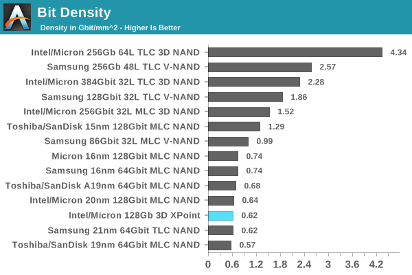
The analysis from TechInsights confirms that 3D XPoint memory is manufactured using a 20nm process, with the same pitch in both the bitline and wordline directions of the memory array. The DRAM market is only just moving beyond this milestone, so comparing the density of 3D XPoint to current DRAM highlights the fundamental capacity advantage 3D XPoint enjoys: around 4.5 times higher density compared to typical 20nm DRAM, and about 3.3 times higher than the most advanced 1Xnm DDR4 on the market. This gap is likely to widen with future generations of 3D XPoint.
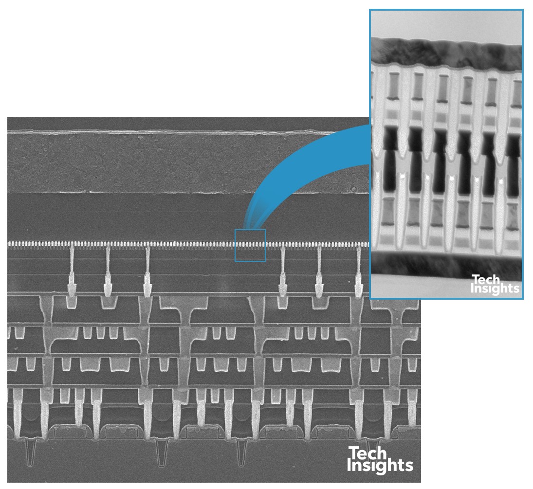
The materials and construction of an individual 3D XPoint memory cell have not been fully analyzed, but it appears to be a phase change memory element with a doped chalcogenide selector switch. The 3D XPoint memory array is constructed between the fourth and fifth metal interconnect layers above the silicon die.
Source: TechInsights


22 Comments
View All Comments
jjj - Saturday, May 27, 2017 - link
This is highly misleading , you focus on density when manufacturing is very different from NAND and DRAM. You do realize that most of your readers don't understand that cost is not just die size. Even you don't seem to understand the difference between costs and pricing. Cost isn't really a factor in how XPoint is priced today.dwrivers - Saturday, May 27, 2017 - link
The article says that die size is a "strong predictor" of cost, which it certainly is.jjj - Saturday, May 27, 2017 - link
Not even close to that when you compare 2 very different things.jjj - Saturday, May 27, 2017 - link
And to state the obvious, since the article fails to do so, XPoint competes with NAND as is lacks the specs to compete with DRAM. If you look at bit density vs Micron's 64L 256GB, 4.34 vs 0.62, that's 7 times.That only gets worse as the 3D NAND architecture is aimed at scaling on the vertical while XPoint isn't. WD/Toshiba likely have a more 3D NAND like architecture for their ReRAM, we'll see soon enough.
As for DRAM, we'll see ,it might go 4F2, might go 3D , might even be replaced by a SCM.
melgross - Sunday, May 28, 2017 - link
It's not supposed to be directly competing with DRAM. That's something some of you posters are making up for yourselves. But it does look that it will compete favorably against DRAM. Performancewise, Intel has said that it won't equal performance, so we've know that from the beginning. But it comes far closer than NAND does, and so, for some purposes it could substitute for more RAM.melgross - Sunday, May 28, 2017 - link
Density and die size are always important. This is also first generation. They're way down on the learning curve. I'd bet that next year, a new board will have 512GB and cost under $1,000. That would be about half the cost of today's board. I do t see anything other that larger sizes and lower costs in the future.Will it ever surpass NAND in pricing? Likely it will. When, well we don't know that yet.
I've no doubt that the price is influenced by R&D costs, as pricing always is.
Samus - Saturday, May 27, 2017 - link
I'm excited for this technology, just not right now. Once it's economical and scalable, it could fundamentally revolutionize the way PC's function, altering (or combining) the roles of storage and RAM.hahmed330 - Saturday, May 27, 2017 - link
It probably never will endurance of RAM is almost infinite.Lolimaster - Sunday, May 28, 2017 - link
For consumer use the best application is to simply use it as a dedicated swap file drive + some programs installed on it. 16GB should do it.Swap inside an SSD wears the thing with constant (but small) writes on top of normal usage. When you hit an HDD based swap you feel the pain.
Optanes m.2 need to work on AMD mobos too.
Lolimaster - Sunday, May 28, 2017 - link
With the current DDR4 prices, people are mostly stuck at 8-16GB of total ram, 16GB of optane swap sounds nice.