TSMC: N7+ EUV Process Technology in High Volume, 6nm (N6) Coming Soon
by Anton Shilov on October 8, 2019 2:00 PM EST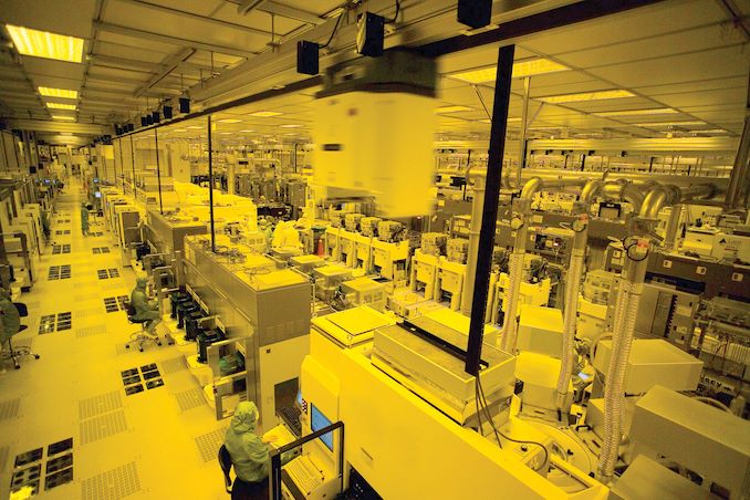
TSMC announced on Monday that its customers have started shipping products based on chips made by TSMC using its N7+ (2nd Generation 7 nm with EUV) process technology that uses extreme ultraviolet lithography (EUVL) for up to four layers. The company also said that its clients are on track to tape out chips to be made using N6 node next year.
When compared to N7 (1st Generation 7 nm) that solely relies on deep ultraviolet lithography, TSMC lists its N7+ process as providing a 15% to 20% higher transistor density as well as 10% lower power consumption at the same complexity and frequency. Furthermore, after less than two quarters in production, TSMC is stating that N7+ now matches N7’s yields, which has been used for over a year now.
Use of EUVL enables TSMC to reduce usage of multipatterning technologies when printing highly complex circuits. This also means that TSMC’s EUV tools can offer output power of greater than 250 watts for day-to-day operations while reaching target goals for availability.
| Advertised PPA Improvements of New Process Technologies Data announced by companies during conference calls, press briefings and in press releases |
|||||||||
| TSMC | |||||||||
| 16FF+ vs 20SOC |
10FF vs 16FF+ |
7FF vs 16FF+ |
7FF vs 10FF |
7FF+ vs 7FF |
6FF vs 7FF |
5FF vs 7FF |
|||
| Power | 60% | 40% | 60% | <40% | 10% | ? | 20% | ||
| Performance | 40% | 20% | 30% | ? | same (?) | ? | 15% | ||
| Area Reduction | none | >50% | 70% | >37% | ~17% | 18% | 45% | ||
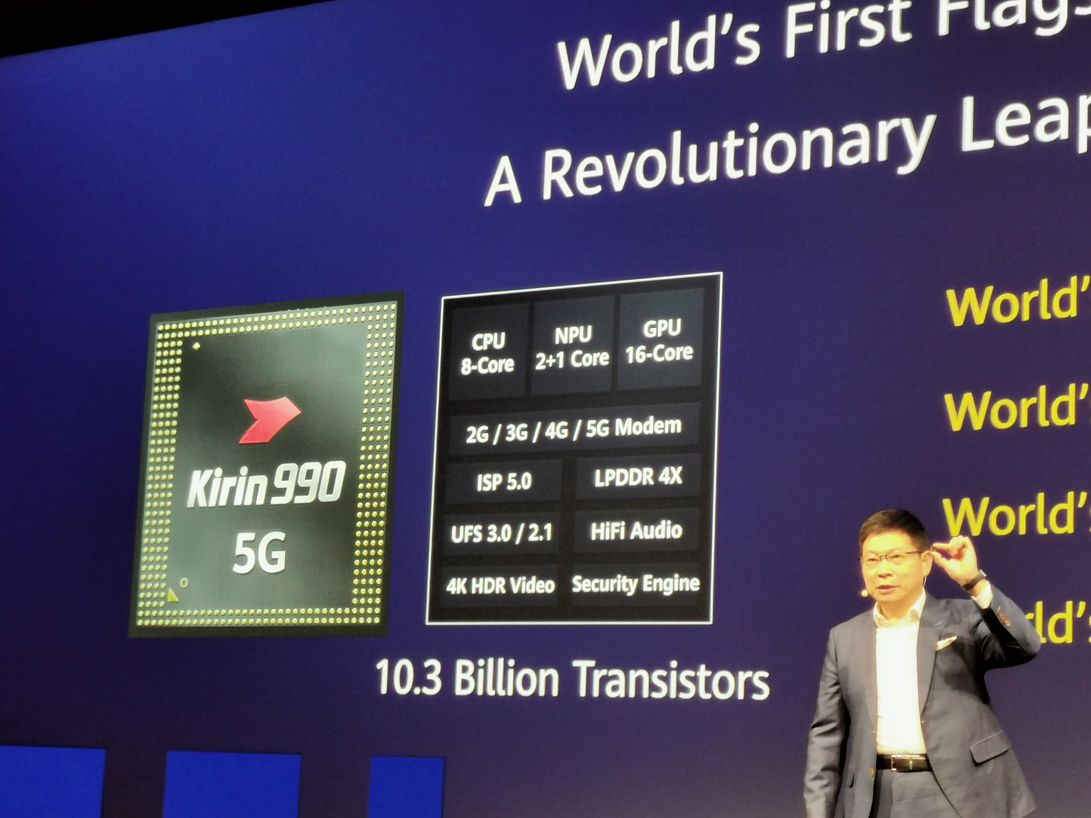
At present, TSMC uses N7+ to produce chips for multiple customers. The most prominent customer of N7+ is Huawei's Hisilicon with the Kirin 990 5G.
TSMC is on track to start risk production of semiconductors using its N6 process technology in the first quarter of 2020 and initiate high-volume production using this node by the end of next year. TSMC’s N6 is a further development of N7 that offers 18% higher transistor density, uses EUVL for up to five layers and enables designers of chips to re-use the same design ecosystem (e.g., tools, IP, etc.), which lowers development costs. By contrast, N7+ uses different design rules, but also provides more benefits than N6 when compared to N7.
Related Reading
- TSMC Announces Performance-Enhanced 7nm & 5nm Process Technologies
- TSMC: Most 7nm Clients Will Transition to 6nm
- TSMC Reveals 6 nm Process Technology: 7 nm with Higher Transistor Density
- TSMC’s 5nm EUV Making Progress: PDK, DRM, EDA Tools, 3rd Party IP Ready
- TSMC: 7nm Now Biggest Share of Revenue
- TSMC: First 7nm EUV Chips Taped Out, 5nm Risk Production in Q2 2019
- TSMC Details 5 nm Process Tech: Aggressive Scaling, But Thin Power and Performance Gains
Source: TSMC


27 Comments
View All Comments
Rudde - Thursday, October 10, 2019 - link
AFAIK, TSMC has the new nodes N7P, N7+, N6 and N5 that are ready in that order. Apple uses N7P for A13. AMD uses N7+ for Zen 3 (4th gen Ryzen). N6 is evolution of N7P. N7+ is better than N6, and N5 trumps both.Krayzieka - Tuesday, October 8, 2019 - link
One thing for sure AMD can lower their price even more with these 7nm euv. I believe up to 5ghz is possible. It million questions on how much zen architecture can improve from here and Lisa Su already mention there are more IPC to squeeze.edzieba - Wednesday, October 9, 2019 - link
"One thing for sure AMD can lower their price even more with these 7nm euv"Every process since 28nm has been cost/transistor go up, not down. This trend is not going to reverse any time soon. Moving to a newer process and 'die shrinking' no longer nets you a cost improvement, and has not for quite some time now.
p1esk - Wednesday, October 9, 2019 - link
EULksec - Tuesday, October 8, 2019 - link
Wait a min. Anton I think this could be wrong.When TSMC say 2nd Generation 7nm, they are referring to N7P, which is an improved version of N7 based on DUV.
The N7+, is based on EUV, and the next step , 2nd generation of that is N6. With additional layers using EUV.
I have yet to see any concrete answer as to Apple using EUV, and since Apple likely to follow TSMC's terminology, 2nd Generation 7nm likely refers to N7P. Which means Apple hasn't adopted EUV yet.
Frenetic Pony - Tuesday, October 8, 2019 - link
Well, no, 6nm is a separate upgrade path from 7nm+. I'm unsure what Apple is using though, did hear they balked at 7nm+.ksec - Wednesday, October 9, 2019 - link
What do you mean by Separate upgrade path.levizx - Thursday, October 10, 2019 - link
Apple is NOT using EUV. And N6 is a more compatible version of N7+.FreckledTrout - Wednesday, October 9, 2019 - link
TSMC publicly announced they are in high volume production of N7+ aka 7nm+.This is easily searchable, https://www.tsmc.com/tsmcdotcom/PRListingNewsActio...
ksec - Wednesday, October 9, 2019 - link
And that by no means N7+ is being used by Apple. Huawei is also N7+.