Qualcomm Announces Snapdragon 8 Gen 1: Flagship SoC for 2022 Devices
by Andrei Frumusanu on November 30, 2021 6:00 PM EST
At this year’s Tech Summit from Hawaii, it’s time again for Qualcomm to unveil and detail the company’s most important launch of the year, showcasing the newest Snapdragon flagship SoC that will be powering our upcoming 2022 devices. Today, as the first of a few announcements at the event, Qualcomm is announcing the new Snapdragon 8 Gen 1, the direct follow-up to last year’s Snapdragon 888.
The Snapdragon 8 Gen 1 follows up its predecessors with a very obvious change in marketing and product naming, as the company is attempting to simplify its product naming and line-up. Still part of the “8 series”, meaning the highest end segment for devices, the 8 Gen 1 resets the previous three-digit naming scheme in favor of just a segment and generation number. For Qualcomm's flagship part this is pretty straightforward, but it remains to be seen what this means for the 7 and 6 series, both of which have upwards of several parts for each generation.
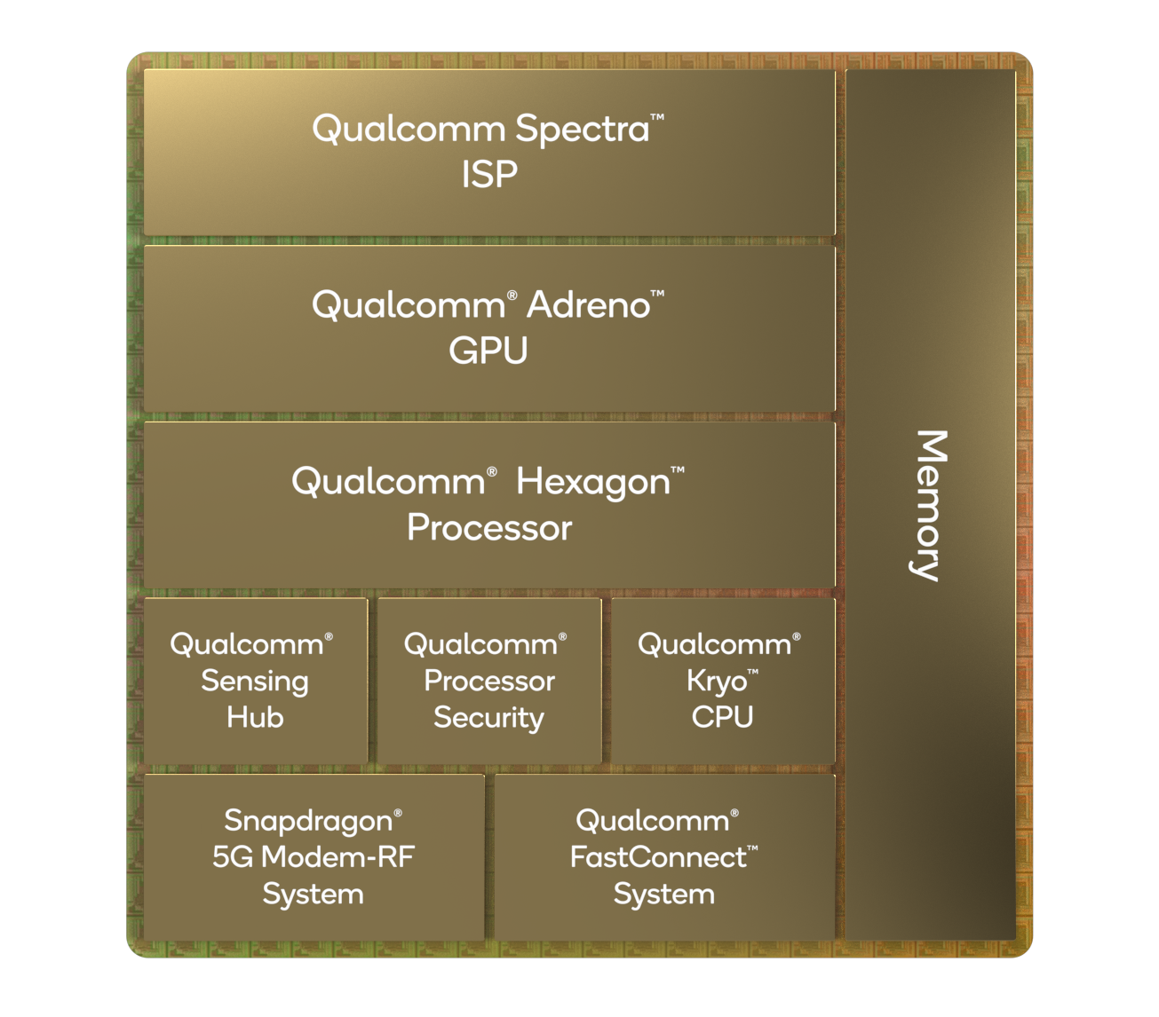
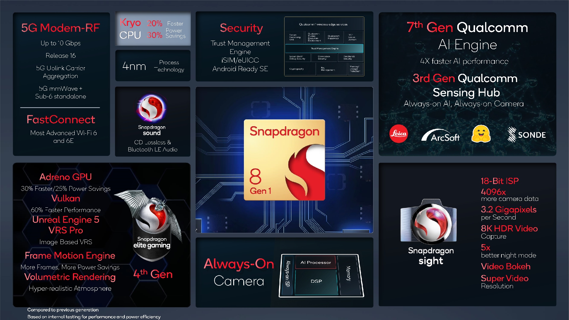
As for the Snapdragon 8 Gen 1, the new chip comes with a lot of new IP: We’re seeing the new trio of Armv9 Cortex CPU cores from Arm, a whole new next-generation Adreno GPU, a massively improved imaging pipeline with lots of new features, an upgraded Hexagon NPU/DSP, integrated X65 5G modem, and all manufactured on a newer Samsung 4nm process node.
The new chip promises large increases in performance and efficiency in a lot of the processing elements, as well as new features enabling new user experiences. Let’s start over the basic specifications and drill down the details that we have on the chip:
| Qualcomm Snapdragon Flagship SoCs 2020-2021 | |||
| SoC |
Snapdragon 8 Gen 1 |
Snapdragon 888 | |
| CPU | 1x Cortex-X2 @ 3.0GHz 1x1024KB pL2 3x Cortex-A710 @ 2.5GHz 3x512KB pL2 4x Cortex-A510 @ 1.80GHz 2x??KB sL2 6MB sL3 |
1x Cortex-X1 @ 2.84GHz 1x1024KB pL2 3x Cortex-A78 @ 2.42GHz 3x512KB pL2 4x Cortex-A55 @ 1.80GHz 4x128KB pL2 4MB sL3 |
|
| GPU | Adreno next-gen | Adreno 660 @ 840MHz | |
| DSP / NPU | Hexagon | Hexagon 780 26 TOPS AI (Total CPU+GPU+HVX+Tensor) |
|
| Memory Controller |
4x 16-bit CH @ 3200MHz LPDDR5 / 51.2GB/s 4MB system level cache |
||
| ISP/Camera | Triple 18-bit Spectra ISP 1x 200MP or 108MP with ZSL or 64+36MP with ZSL or 3x 36MP with ZSL 8K HDR video & 64MP burst capture |
Triple 14-bit Spectra 580 ISP 1x 200MP or 84MP with ZSL or 64+25MP with ZSL or 3x 28MP with ZSL 4K video & 64MP burst capture |
|
| Encode/ Decode |
8K30 / 4K120 10-bit H.265 Dolby Vision, HDR10+, HDR10, HLG 720p960 infinite recording |
||
| Integrated Modem | X65 integrated (5G NR Sub-6 + mmWave) DL = 10000 Mbps UL = 3000 Mbps |
X60 integrated (5G NR Sub-6 + mmWave) DL = 7500 Mbps UL = 3000 Mbps |
|
| Mfc. Process | Samsung 4nm (unspecified) |
Samsung 5nm (5LPE) |
|
CPUs: Cortex-X2 and Armv9 siblings
Starting off with the CPUs of the new Snapdragon 8 Gen 1 (I’ll shorthand it as S8g1 here and there): This is Qualcomm’s first chip featuring the new Armv9 generation of CPU IPs from Arm, which includes the Cortex-X2, Cortex-A710, and Cortex-A510 in a big, middle, and little setup. Qualcomm continues to use a 1+3+4 core count, a setup that’s been relatively successful for the designers over the past few years and iterations ever since the Snapdragon 855.
The Cortex-X2 core of the new chip clocks in at 3.0GHz, which is a tad higher than the 2.84GHz clock of the X1 core on the Snapdragon 888. This was actually a bit surprising to me, as I hadn’t expected much in the way of clock increases this generation, but it’s nice to see Arm vendors now routinely achieving this. For context, MediaTek’s recently announced Dimensity 9000 achieves 3.05GHz on its X2 core, however that’s on a TSMC N4 node. In contrast, Qualcomm manufactures the Snapdragon 8 Gen 1 on a Samsung 4nm node. The company wouldn’t confirm if it’s a 4LPE variant or something more custom, hence why we’re leaving it as a “4nm” node description in the specification table.
What is most surprising about the X2 core is that Qualcomm is claiming 20% faster performance or 30% power savings, the latter figure being especially intriguing. Samsung Foundry only describe a 16% reduction in power in going from a 5nm to 4nm node, and obviously 30% is significantly better than what the process node promises. We asked Qualcomm what kind of improvements lead to such a large power decrease; however, the company wouldn’t specify any details. I particularly asked if the new X2 cores have their own voltage domain (Previous Snapdragon 1+3 big+middle implementations shared the same voltage rail), but the company wouldn’t even confirm if this was the case or not. Arm had noted that the X2 can have quite lower power at the same peak performance point of the X1, if Qualcomm’s marketing materials refer to such a comparison, then the numbers might make sense.
The X2 core is configured with 1MB of L2 cache, while the three Cortex-X710 cores have 512KB each. The middle cores here are clocked slightly higher at 2.5GHz this year, a little 80MHz jump over the previous generation. Usually, the middle cores pay more attention to the power budget, so maybe this slightly increase does represent more accurately the process node improvements.
Lastly, the new chip also makes use of four Cortex-A510 cores at 1.8GHz. Unlike the Dimensity 9000 from a couple of weeks back, Qualcomm does make use of Arm’s new “merged-core” approach of the new microarchitecture, meaning that the chip actually has two Cortex-A510 complexes with two cores each, sharing a common NEON/SIMD pipeline and L2 cache. The merged core approach is meant to achieve better area efficiency. Qualcomm rationalized the approach by saying that in everyday use cases with fewer threads active and overall low activity, having a single core able to access a larger L2 cache shared by two cores can result in better performance and efficiency. Unfortunately even while making this comment, the company wouldn’t actually detail what the L2 size was, whether it’s 512KB or 256KB – if it’s the latter, then the configuration definitely isn’t as aggressive as the Dimensity 9000.
The new Armv9 CPU IPs from Arm also came with a new generation DSU (DynamiQ Shared Unit, the cluster IP) which the new Snapdragon makes use of. Qualcomm here opted for a 6MB L3 cache size, noting that this was a decision in balancing out system performance across target workloads.
As for system caches, Qualcomm mentioned that the chip remains unchanged with a 4MB cache, and the memory controllers are still 3200MHz LPDDR5 (4x 16bit channels). It’s to be noted that, as with last year’s Snapdragon 888, the CPUs no longer have access to the system cache, in order to improve DRAM latency. We can’t help but make comparisons to MediaTek’s Dimensity 9000, which likely will have worse DRAM latency, but also offer up to 14MB of shared caches to the CPUs versus just 6MB on the Snapdragon 8 Gen 1. How the two chips will compare to each other remains to be seen in actual commercial devices.
GPU: New Adreno architecture with no name
Back in the day, Qualcomm’s Adreno GPU architectures were easy to identify in terms of their family as well as performance levels. Particularly on the architecture side, the Adreno 600 series started off with the Adreno 630 in the Snapdragon 845 a few years ago, but unlike in previous iterations from the 400- and 500 series, we remained with that high-level description up until the Snapdragon 888 series.
The Snapdragon 8 Gen 1 here changes things, and frankly, Qualcomm did a quite horrible job at marketing what they have this time around. The new GPU name completely drops any model number, and as such doesn’t immediately divulge that it’s part of a larger microarchitecture shift that in the past would have been marketed as a new Adreno series.
Qualcomm notes that from an extremely high-level perspective, the new GPU might look similar to the previous generations, however there are large architectural changes included that are meant to improve performance and efficiency. Qualcomm gave examples such as concurrent processing optimizations that are meant to give large boosts in performance to real-world workloads that might not directly show up in benchmarks. Another example was that the GPU’s “GMEM” saw large changes this generation, such as an increase of 33% of the cache (to 4MB), and now being both a read & write cache rather than just a writeback cache for DRAM traffic optimizations.
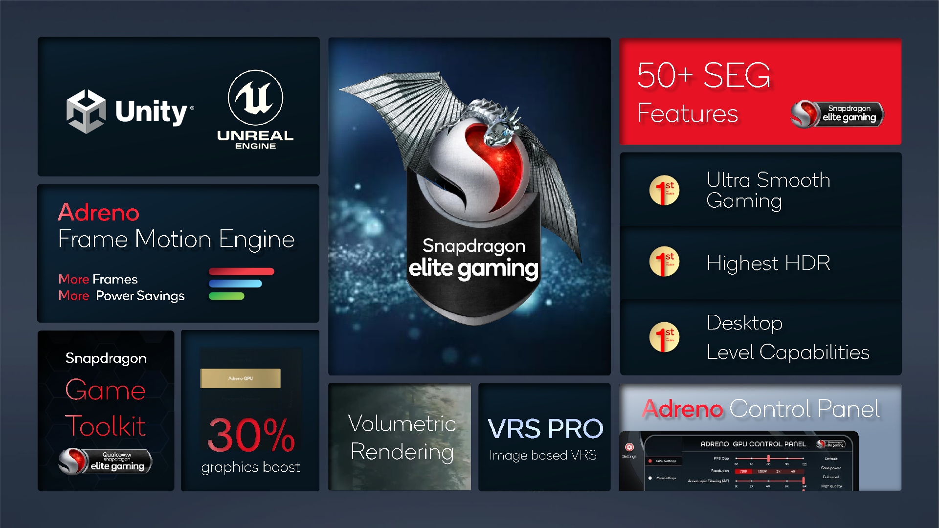
The high-level performance claims are 30% faster peak performance, or 25% power reduction at the same performance as the Snapdragon 888. Qualcomm also uncharacteristically commented on the situation of peak power figures and the current situation in the market. Last year, Qualcomm rationalized the Snapdragon 888’s high peak GPU power figures by noting that this is what vendors had demanded in response to what we saw from other players, notably Apple, and that vendors would be able to achieve better thermal envelopes in their devices. Arguably, this strategy ended up as being quite disastrous and negative in terms of perception for Qualcomm, and I feel that in this year’s briefing we saw Quaclomm attempt to distance themselves more from the situation, largely by outright saying that the only point of such peak performance and power figures is for vendors to achieve higher first-run benchmarking numbers.
Unfortunately, unlike Apple, who actually use their GPU’s peak performance figures in transient compute workloads such as camera processing, currently the Android ecosystem just doesn’t make any advanced use of GPU compute. This admission was actually a breath of fresh air and insight into the situation, as it’s been something I’ve especially noted in our Kirin 9000, Snapdragon 888 and Exynos 2100 and Tensor deep-dives in criticizing all the new chips. It’s an incredibly stupid situation that, as long as the media continues to put weight on peak performance figures, won’t be resolved any time soon, as the chip vendors will have a hard time saying no to their customer’s requests to operate the silicon in this way.
Qualcomm states that one way to try to alleviate this new focus on peak performance is to change the way the GPU performance and power curve behaves. The team stated that they’ve gone in to change the architecture to try to flatten the curve, to not only achieve those arguably senseless peak figures, but actually focus on making larger improvements in the 3-5W power range, a range where the Snapdragon 888 last year didn’t significantly improve upon the Snapdragon 865.
That being said, even with a 25% decrease in power at similar Snapdragon 888 performance, the new Snapdragon 8 Gen 1 likely still won’t be able to compete against Apple’s A14 or A15 chips. MediaTek’s Dimensity 9000 also should also be notably more efficient than the new Snapdragon at equal performance levels given the claimed efficiency figures, so it still looks like Qualcomm’s choice of going with a Samsung process node, even this new 4nm one, won’t close the gap to the TSMC competitors.


219 Comments
View All Comments
Kangal - Friday, December 3, 2021 - link
The Cortex-X1 isn't really a performance core from the ground up, it's a "medium core" that's been tweaked/beefed up, so of course it will have disadvantages to something else, like Apple's Firestorm or Nuvia's cores.The Cortex-X2 design is mostly recycled from the Cortex-X1/Cortex-A78 (and Cortex-A710). And if you really look at it, it's all part of the same Cortex-A76 family. This is ARM's first attempt to get the ARMv9 protocol out there, that aspect alone takes resources away from development. Their performance and efficiency projections for next year have been a let down. That's the context you need to remember.
The Cortex-X3 is supposed to be designed by ARM's European team, and they have a stronger track record than their US Team. So I expect good things. On top of that, they're supposed to start on a new platform; eg Cortex-A730. I believe the difference will be a kin to the Cortex-A57 versus Cortex-A72. So it will be worth waiting for.
With that said, Apple's A15 isn't too far from their A14 and A13 processors. Whilst the X1 and X2 failed to catch up to the Apple A13... I do think the X3 will catch up and potentially surpass it. With the point being that Apple has the new lead with the Apple A16.
The Nuvia cores have been in development for some time. Obviously it's built with ARMv8 in mind. And they do have silicon pressed and sampled already, ie Working Prototypes. And based on the information we know, their Nuvia Cores are better than the Apple A15 in the labs. But now they will have to go back, tweak it, and covert to ARMv9. Again that will take time of the development, and potentially less optimised design in the interim.
Software Support is the part which Apple wins. It's all-round better. Not only can they support it longer, but businesses and developers trust that ecosystem, which means it will get priority for development and for optimisation. The other point is that Apple's software is very advanced: Swift and Metal are actually pretty awesome, and their SDK is the Gold Standard in the industry. Sure you have certain limitations, but within the boundary the software and hardware meld much closer. It's the result of throwing billions of dollars, thousands of in-house developers, and years of experience.
A Qualcomm-Nuvia product has no answer for that. If they try AndroidOS, they will have lots of compromises. Whilst Microsoft is usually better, lately they've done a poor job with W-ART, Windows-on-ARM, and Windows 11. So I don't expect a Q-Nuvia laptop doing as well, so they will lose some performance and efficiency there again to the likes of Apple's iPad/Macbook.
tkSteveFOX - Wednesday, December 1, 2021 - link
It's clear ARM designs have hit a brick wall. The improvements in architecture just aren't enough when compared to Apple's. While Android phones have more mature ISP and modems, Job's lot silicon is at least a generation if not two ahead in performance and efficiency.Android phones now regularly costing more or as much as iphones means you as a customer are more likely to choose Apple in the longer run.
Wilco1 - Wednesday, December 1, 2021 - link
A 20% yearly improvement is hardly a brick wall. While the L2/L3 caches are still on the small side (especially when compared to Dimensity 9000), this should narrow the gap. You're not going to notice the difference though. Most phones use far older and slower cores (Samsung just announced a phone with 1.2/1.6GHz Cortex-A55!!!), and there a 10-20% difference will be very noticeable. But at the high-end? Absolutely not.As for efficiency, my S21 Ultra has the same battery life as iPhone 13 Pro according to AnandTech. And I paid far less for it. As a consumer that matters to me more than whether or not the iPhone is faster on SPEC or Geekbench.
high3r - Wednesday, December 1, 2021 - link
Wow, 3095 mAh vs 5000 mAh. That's something then. :)Wilco1 - Wednesday, December 1, 2021 - link
Design capacity of S21 Ultra is 4855 mAh, estimated capacity around 4700 mAh according to Accubattery. It lasts 4 to 5 days on a full charge which is exceptionally good.iPhones use a huge SoC with lots of cache on the most advanced process which allows for a smaller battery, while Android phones use a much smaller SoC on a less advanced process and a larger battery instead.
TheinsanegamerN - Thursday, December 2, 2021 - link
It will be something in 2 years when the samsung can still go for more then 4 hours without keeling over. The iphone, OTOH......mode_13h - Wednesday, December 1, 2021 - link
> While the L2/L3 caches are still on the small side (especially when compared to Dimensity 9000)Isn't the 9000 aimed primarily or exclusively at laptops? Why compare it to a phone SoC, then? Phones have smaller batteries and worse cooling.
Wilco1 - Wednesday, December 1, 2021 - link
Eh what?!? This clearly states smartphone repeatedly - in huge letters, so impossible to miss... https://i.mediatek.com/summit-dimensity9000For laptops there is Cortex-A78C and Cortex-X1C.
mode_13h - Wednesday, December 1, 2021 - link
Okay, my bad. I thought I remembered something about it being a Chromebook SoC.name99 - Monday, December 6, 2021 - link
You'd think so ("you won't notice the difference") but you do.I'm happy with my iPhone XS (A12) but when I used a friend's iPhone 13 Pro (A15) the extra speed was noticeable. I couldn't say WHERE the difference lies; my phone never stutters or glitches in animation and apps launch basically instantly. But even so you can feel that the iPhone13 Pro is faster, and not just subtly so.
Maybe it's in the 120Hz? But even so, you need a SoC that can keep that 120Hz fed while never glitching...