Intel Iris Pro 5200 Graphics Review: Core i7-4950HQ Tested
by Anand Lal Shimpi on June 1, 2013 10:01 AM ESTHaswell GPU Architecture & Iris Pro
In 2010, Intel’s Clarkdale and Arrandale CPUs dropped the GMA (Graphics Media Accelerator) label from its integrated graphics. From that point on, all Intel graphics would be known as Intel HD graphics. With certain versions of Haswell, Intel once again parts ways with its old brand and introduces a new one, this time the change is much more significant.
Intel attempted to simplify the naming confusion with this slide:
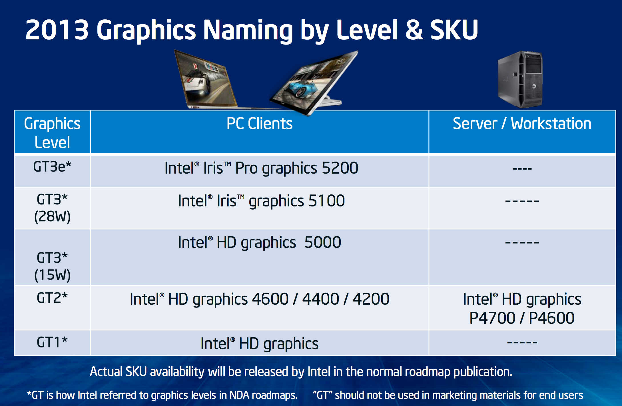
While Sandy and Ivy Bridge featured two different GPU implementations (GT1 and GT2), Haswell adds a third (GT3).
Basically it boils down to this. Haswell GT1 is just called Intel HD Graphics, Haswell GT2 is HD 4200/4400/4600. Haswell GT3 at or below 1.1GHz is called HD 5000. Haswell GT3 capable of hitting 1.3GHz is called Iris 5100, and finally Haswell GT3e (GT3 + embedded DRAM) is called Iris Pro 5200.
The fundamental GPU architecture hasn’t changed much between Ivy Bridge and Haswell. There are some enhancements, but for the most part what we’re looking at here is a dramatic increase in the amount of die area allocated for graphics.
All GPU vendors have some fundamental building block they scale up/down to hit various performance/power/price targets. AMD calls theirs a Compute Unit, NVIDIA’s is known as an SMX, and Intel’s is called a sub-slice.
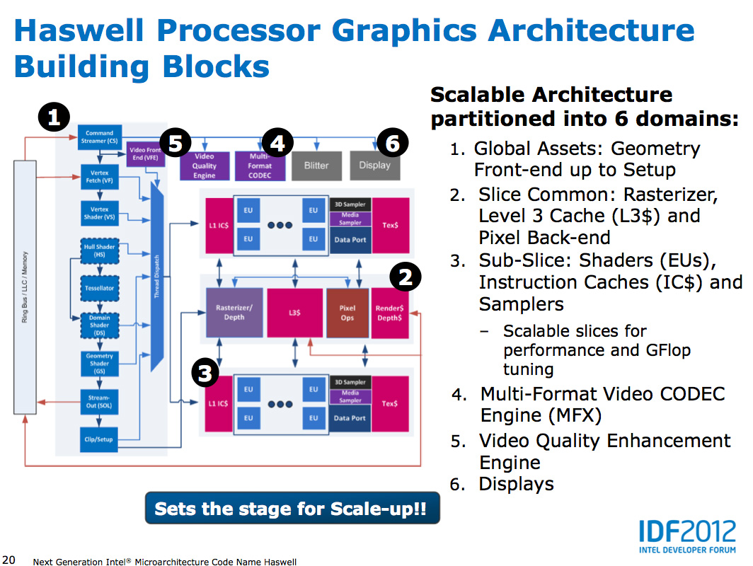
In Haswell, each graphics sub-slice features 10 EUs. Each EU is a dual-issue SIMD machine with two 4-wide vector ALUs:
| Low Level Architecture Comparison | ||||||||||||||||
| AMD GCN | Intel Gen7 Graphics | NVIDIA Kepler | ||||||||||||||
| Building Block | GCN Compute Unit | Sub-Slice | Kepler SMX | |||||||||||||
| Shader Building Block | 16-wide Vector SIMD | 2 x 4-wide Vector SIMD | 32-wide Vector SIMD | |||||||||||||
| Smallest Implementation | 4 SIMDs | 10 SIMDs | 6 SIMDs | |||||||||||||
| Smallest Implementation (ALUs) | 64 | 80 | 192 | |||||||||||||
There are limitations as to what can be co-issued down each EU’s pair of pipes. Intel addressed many of the co-issue limitations last generation with Ivy Bridge, but there are still some that remain.
Architecturally, this makes Intel’s Gen7 graphics core a bit odd compared to AMD’s GCN and NVIDIA’s Kepler, both of which feature much wider SIMD arrays without any co-issue requirements. The smallest sub-slice in Haswell however delivers a competitive number of ALUs to AMD and NVIDIA implementations.
Intel had a decent building block with Ivy Bridge, but it chose not to scale it up as far as it would go. With Haswell that changes. In its highest performing configuration, Haswell implements four sub-slices or 40 EUs. Doing the math reveals a very competent looking part on paper:
| Peak Theoretical GPU Performance | ||||||||||||||||
| Cores/EUs | Peak FP ops per Core/EU | Max GPU Frequency | Peak GFLOPs | |||||||||||||
| Intel Iris Pro 5100/5200 | 40 | 16 | 1300MHz | 832 GFLOPS | ||||||||||||
| Intel HD Graphics 5000 | 40 | 16 | 1100MHz | 704 GFLOPS | ||||||||||||
| NVIDIA GeForce GT 650M | 384 | 2 | 900MHz | 691.2 GFLOPS | ||||||||||||
| Intel HD Graphics 4600 | 20 | 16 | 1350MHz | 432 GFLOPS | ||||||||||||
| Intel HD Graphics 4000 | 16 | 16 | 1150MHz | 294.4 GFLOPS | ||||||||||||
| Intel HD Graphics 3000 | 12 | 12 | 1350MHz | 194.4 GFLOPS | ||||||||||||
| Intel HD Graphics 2000 | 6 | 12 | 1350MHz | 97.2 GFLOPS | ||||||||||||
| Apple A6X | 32 | 8 | 300MHz | 76.8 GFLOPS | ||||||||||||
In its highest end configuration, Iris has more raw compute power than a GeForce GT 650M - and even more than a GeForce GT 750M. Now we’re comparing across architectures here so this won’t necessarily translate into a performance advantage in games, but the takeaway is that with HD 5000, Iris 5100 and Iris Pro 5200 Intel is finally walking the walk of a GPU company.
Peak theoretical performance falls off steeply as soon as you start looking at the GT2 and GT1 implementations. With 1/4 - 1/2 of the execution resources as the GT3 graphics implementation, and no corresponding increase in frequency to offset the loss the slower parts are substantially less capable. The good news is that Haswell GT2 (HD 4600) is at least more capable than Ivy Bridge GT2 (HD 4000).
Taking a step back and looking at the rest of the theoretical numbers gives us a more well rounded look at Intel’s graphics architectures :
| Peak Theoretical GPU Performance | ||||||||||||||||
| Peak Pixel Fill Rate | Peak Texel Rate | Peak Polygon Rate | Peak GFLOPs | |||||||||||||
| Intel Iris Pro 5100/5200 | 10.4 GPixels/s | 20.8 GTexels/s | 650 MPolys/s | 832 GFLOPS | ||||||||||||
| Intel HD Graphics 5000 | 8.8 GPixels/s | 17.6 GTexels/s | 550 MPolys/s | 704 GFLOPS | ||||||||||||
| NVIDIA GeForce GT 650M | 14.4 GPixels/s | 28.8 GTexels/s | 900 MPolys/s | 691.2 GFLOPS | ||||||||||||
| Intel HD Graphics 4600 | 5.4 GPixels/s | 10.8 GTexels/s | 675 MPolys/s | 432 GFLOPS | ||||||||||||
| AMD Radeon HD 7660D (Desktop Trinity, A10-5800K) | 6.4 GPixels/s | 19.2 GTexels/s | 800 MPolys/s | 614 GFLOPS | ||||||||||||
| AMD Radeon HD 7660G (Mobile Trinity, A10-4600M) | 3.97 GPixels/s | 11.9 GTexels/s | 496 MPolys/s | 380 GFLOPS | ||||||||||||
Intel may have more raw compute, but NVIDIA invested more everywhere else in the pipeline. Triangle, texturing and pixel throughput capabilities are all higher on the 650M than on Iris Pro 5200. Compared to AMD's Trinity however, Intel has a big advantage.


177 Comments
View All Comments
boe - Monday, June 3, 2013 - link
As soon as intel CPUs have video performance that exceeds NVidia and AMD flagship video cards I'll get excited. Until then I think of them as something to be disabled on workstations and to be tolerated on laptops that don't have better GPUs on board.MySchizoBuddy - Monday, June 3, 2013 - link
So Intel just took the OpenCL crown. Never thought this day would come.prophet001 - Monday, June 3, 2013 - link
I have no idea whether or not any of this article is factually accurate.However, the first page was a treat to read. Very well written.
:)
Teemo2013 - Monday, June 3, 2013 - link
Great success by Intel.4600 is near GT630 and HD4650 (much better than 6450 which sells for $15 at newegg)
5200 is better than GT640 and HD 6670 (currently sells like $50 at newegg)
Intel's intergrated used to be worthless comparing with discret cards. It slowly catches up during the past 3 years, and now 5200 is beating a $50 card. Can't wait for next year!
Hopefully this will finally push AMD and Nvidia to come up with meaningful upgrade to their low level product lines.
Cloakstar - Monday, June 3, 2013 - link
A quick check for my own sanity:Did you configure the A10-5800K with 4 sticks of RAM in bank+channel interleave mode, or did you leave it memory bandwidth starved with 2 sticks or locked in bank interleave mode?
The numbers look about right for 2 sticks, and if that is the case, it would leave Trinity at about 60% of its actual graphics performance.
I find it hard to believe that the 5800K is about a quarter the performace per watt of the 4950HQ in graphics, even with the massive, server-crushing cache.
andrerocha - Monday, June 3, 2013 - link
is this new cpu faster than the 4770k? it sure cost more?zodiacfml - Monday, June 3, 2013 - link
impressive but one has to take advantage of the compute/quick sync performance to justify the increase in price over the HD 4600ickibar1234 - Tuesday, June 4, 2013 - link
Well, my Asus G50VT laptop is officially obsolete! A Nvidia 512MB GDDR3 9800gs is completely pwned by this integrated GPU, and, the CPU is about 50-65% faster clock for clock to the last generation Core 2 Duo Penryn chips. Sure, my X9100 can overclock stably to 3.5GHZ but this one can get close even if all cores are fully taxed.Can't wait to see what the Broadwell die shrink brings, maybe a 6-core with Iris or a higher clocked 4-core?
I too see that dual core versions of mobile Haswell with this integrated GPU would be beneficial. Could go into small 4.5 pounds laptops.
AMD.....WTH are you going to do.
zodiacfml - Tuesday, June 4, 2013 - link
AMD has to create a Crystalwell of their own. I never thought Intel could beat them to it since their integrated GPUs always has needed bandwidth ever since.Spunjji - Tuesday, June 4, 2013 - link
They also need to find a way past their manufacturing process disadvantage, which may not be possible at all. We're comparing 22nm Apples to 32/28nm Pears here; it's a relevant comparison because those are the realities of the marketplace, but it's worth bearing in mind when comparing architecture efficiencies.