Original Link: https://www.anandtech.com/show/8216/samsung-ssd-850-pro-128gb-256gb-1tb-review-enter-the-3d-era
Samsung SSD 850 Pro (128GB, 256GB & 1TB) Review: Enter the 3D Era
by Kristian Vättö on July 1, 2014 10:00 AM EST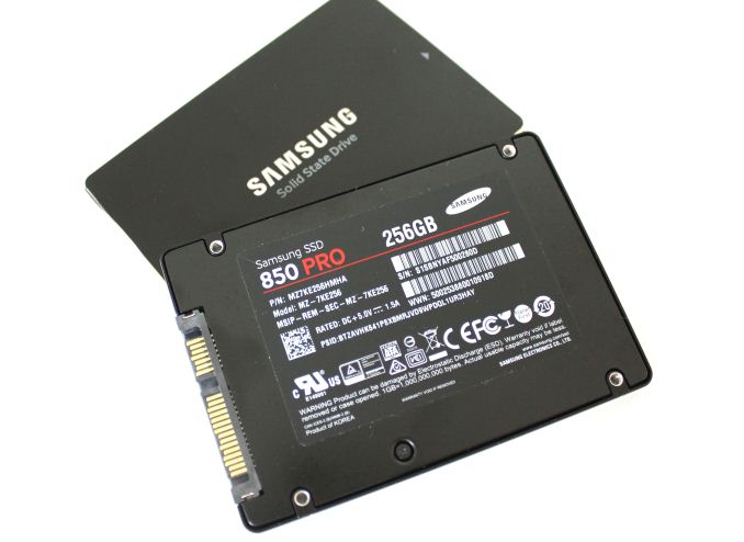
Over the last three years, Samsung has become one of the most dominant players in the SSD industry. Samsung's strategy has been tight vertical integration ever since the beginning, which gives Samsung the ability to be in the forefront of new technologies. That is a massive advantage because ultimately all the parts need to be designed and optimized to work properly together. The first fruit of Samsung's vertical integration was the SSD 840, which was the first mass produced SSD to utilize TLC NAND and gave Samsung a substantial cost advantage. Even today, the SSD 840 and its successor, the 840 EVO, are still the only TLC NAND based SSDs shipping in high volume. Now, two years later, Samsung is doing it again with the introduction of the SSD 850 Pro, the world's first consumer SSD with 3D NAND.
For years it has been known that the scalability of traditional NAND is coming to an end. Every die shrink has been more difficult than the previous as the endurance and performance have decreased with every node, making it less and less efficient to scale the size down. Scaling below 20nm was seemed as a major obstacle but the industry was able to cross that with some clever innovations in the NAND design. However, the magic hat is now running out of tricks and a more signficant change to the NAND design is required to keep scaling the cost.
The present solution to the scalability problem is 3D NAND, or V-NAND as Samsung calls it. Traditionally NAND and other semiconductors are scaled horizontally along the X and Y axes but due to the laws of physics, there is a limit of how small the transistors can be made. To solve the problem, 3D NAND introduces a Z-axis i.e. a vertical dimension. Instead of cramming transistors horizontally closer and closer to each other, 3D NAND stacks layers of transistors on top of each other. I will be going through the structure and characteristics of 3D NAND in detail over the next few pages.
By stacking transistors (i.e. cells when speaking about NAND) vertically, Samsung is able to relax the process node back to a much more convenient 40nm. When there are 32 cells on top of each other, it is obvious that there is no need for a 10nm-class node because the stacking increases the density, allowing production costs to scale lower. As we have seen with the history of NAND die shrinks, a higher process node provides more endurance and higher performance, which is what the 850 Pro and V-NAND is all about.
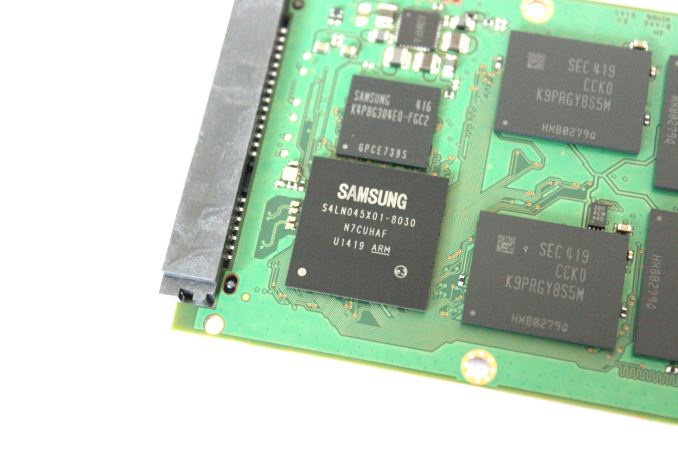
Fundamentally the only change in the 850 Pro is the switch to V-NAND. The interface is still SATA 6Gbps and the controller is the same triple-core MEX from the 840 EVO, although I am still waiting to hear back from Samsung whether the clock speed is the same 400MHz. The firmware, on the other hand, has gone through a massive overhaul to adopt the characteristics of V-NAND. With shorter read, program and erase latencies and higher endurance, the firmware needs to be properly optimized or otherwise the full benefits of V-NAND cannot be utilized.
I bet many of you would have liked to see the 850 Pro move to the PCIe interface but I understand Samsung's decision to hold off with PCIe for a little while longer. The market for aftermarket PCIe SSDs is still relatively small as the PC industry is figuring out how to adopt the new interface, so for the time being Samsung is fine with watching from the side. The XP941 is and will continue to be available to the PC OEMs but for now Samsung will be keeping it that way. From what I have heard, Samsung could bring the XP941 to the retail market rather quickly if needed but Samsung has always been more interested in the high volume mainstream market instead of playing in the niches.
| Samsung SSD 850 Pro Specifications | ||||
| Capacity | 128GB | 256GB | 512GB | 1TB |
| Controller | Samsung MEX | |||
| NAND | Samsung 2nd Gen 86Gbit 40nm MLC V-NAND | |||
| DRAM (LPDDR2) | 256MB | 512MB | 512MB | 1GB |
| Sequential Read | 550MB/s | 550MB/s | 550MB/s | 550MB/s |
| Sequential Write | 470MB/s | 520MB/s | 520MB/s | 520MB/s |
| 4KB Random Read | 100K IOPS | 100K IOPS | 100K IOPS | 100K IOPS |
| 4KB Random Write | 90K IOPS | 90K IOPS | 90K IOPS | 90K IOPS |
| Power | 2mW (DevSLP) / 3.3W (read) / 3.0W (write) | |||
| Encryption | AES-256, TCG Opal 2.0 & IEEE-1667 (eDrive supported) | |||
| Endurance | 150TB | |||
| Warranty | 10 years | |||
| Availability | July 21st | |||
The performance figures in the table above give us the first glimpse of what V-NAND is capable of. Typically modern 128GB SSDs are only good for about 300MB/s but the 850 Pro is very close to saturating the SATA 6Gbps bus even at the smallest capacity. This is due to the much lower program times of V-NAND because write performance has been bound by NAND performance for quite some time now.
| Endurance Comparison of High-End SSDs | |||
| Samsung SSD 850 Pro | Intel SSD 730 | SanDisk Extreme Pro | OCZ Vector 150 |
| 150TB |
91TB (240GB) 128TB (480GB) |
80TB | 91TB |
The other major improvement from V-NAND is the endurance. All capacities, including the smallest 128GB, are rated at 150TB, which is noticeably higher than what any other consumer-grade SSD offers. Moreover, Samsung told me that the endurance figure is mainly meant to separate the 850 Pro from the enterprise drives to guide enterprise clients to the more appropriate (and expensive) drives as the 850 Pro does not have power loss protection or end-to-end data protection for example. However, I was told that the warranty is not automatically denied if 150TB is reached under a client workload. In fact, Samsung said that they have a 128GB 850 Pro in their internal testing with over eight petabytes (that is 8,000TB) of writes and the drive still keeps going, so I tip my hat to the person who is able to wear out an 850 Pro in a client environment during my lifetime.
Another interesting aspect of V-NAND is its odd capacity per die. Traditionally NAND capacies have come in powers of two, such as 64Gbit and 128Gbit, but with V-NAND Samsung is putting an end to that trend. The second generation 32-layer V-NAND comes in at 86Gbit or 10.75GB if you prefer the gigabyte form. I will be covering the reason behind that in more detail when we look at V-NAND more closely in the next few pages but as far as I know there has never been a strict rule as to why the capacities have scaled in powers of two. I believe it is just a relic from the old days that has stayed in the memory industry because deep down binary is based on powers of two but the abnormal die capacity should have no effect on the operation of the NAND or the SSD as long as everything is optimized for it.
| NAND Configurations | ||||
| 128GB | 256GB | 512GB | 1TB | |
| # of NAND Packages | 4 (?) | 4 | 8 (?) | 8 |
| Package Configurations |
2 x 4 x 86Gbit 2 x 2 x 86Gbit |
2 x 8 x 86Gbit 2 x 4 x 86Gbit |
4 x 8 x 86Gbit 4 x 4 x 86Gbit |
4 x 16 x 86Gbit 4 x 8 x 86Gbit |
| Raw NAND Capacity | 129GiB | 258GiB | 516GiB | 1032GiB |
| Over-Provisioning | 7.6% | 7.6% | 7.6% | 7.6% |
Due to the odd die capacity, the die configurations are also quite unusual. I found two different capacity packages inside my review samples and with Samsung’s NAND part decoder I was able to figure out the die configurations for each capacity. Unfortunately, Samsung did not send us the 512GB model and I could not get the 128GB model open as Samsung uses pentalobe Torx screws and I managed to wear out the screw while trying to open it with an inappropriate screw driver (it worked for the other models, though), so thus there are question marks at those capacities in the table. However, this should not impact the raw NAND capacities as long as all capacities follow the same 7.6% over-provisioning trend but the package configurations may be different. I will provide an update once I receive a confirmation from Samsung regarding the exact configurations for each capacity.
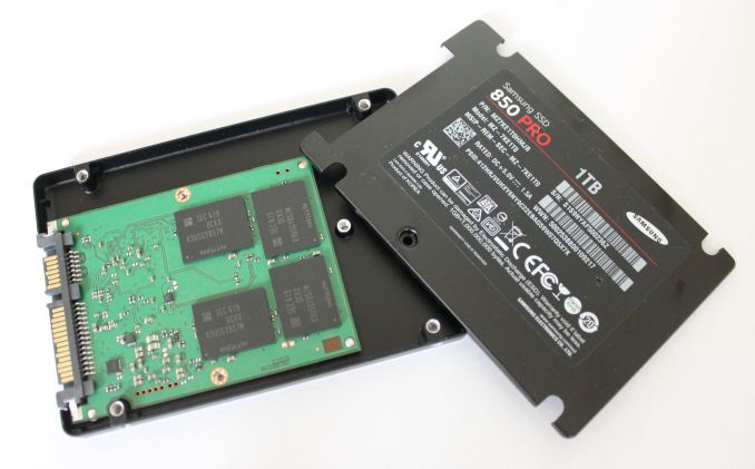
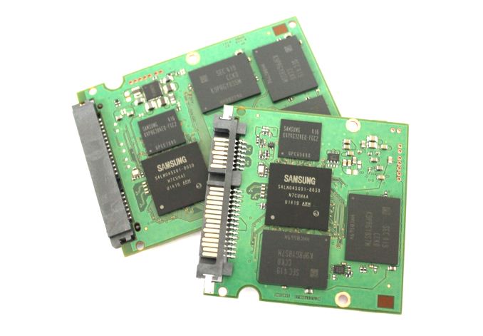
The 850 Pro also switches to smaller PCB designs. The PCB in the 1TB model populates around two thirds of the area of the chassis, while the 256GB PCB comes in at even smaller size. The reason for the different PCB sizes is the amount of NAND packages as the 256GB only has four, whereas to achieve the capacity of 1TB eight NAND packages are required.
Why We Need 3D NAND
For years, it has been known that traditional NAND (i.e. 2D NAND) is running on its last legs. Many analysts predicted that we would not see NAND scaling below 20nm because the reliability would simply be too low to make such a small lithography feasible. However, thanks to some clever engineering on both hardware and firmware sides NAND has scaled to 15nm without any significant issues but now the limit has been reached for real. To understand the limits of 2D NAND scaling, let's say hello to our old good friend Mr. N-channel MOSFET.
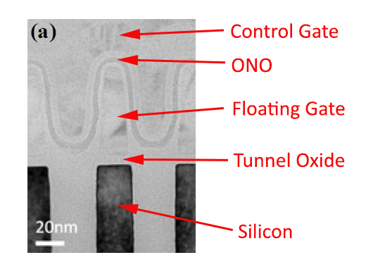
Unfortunately the diagram above is a bit too simplified to truly show what we need, so let's look at a real cross-section photo instead:
Let me walk you through the structure first. At the top is the control gate, which is a part of a structure known as a wordline. In a standard NAND design the control gate wraps around the floating gate and the two gates are separated by an insulating oxide-nitride-oxide layer (i.e. ONO), which is sometimes called Inter Poly Dielectric (IPD). Under the floating gate is the tunnel oxide, which is also an insulator, followed by the silicon substrate that acts as the bitline.
The reason why the control gate is wrapped around the floating gate is to maximize capacitance between the two. As you will soon learn, the capacitance between the gates is the key factor in NAND as it means that the control gate can control the floating gate.
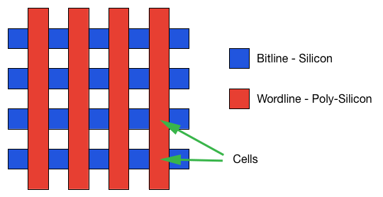
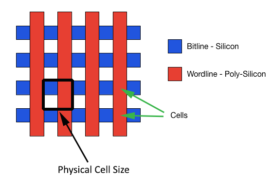
The purpose of bitlines and wordlines can be rather difficult to understand when looking at a cross-section, so here is what it all looks like from the top. Basically, bitlines and wordlines are just lines going in perpendicular directions and the floating gate and other materials reside between them.
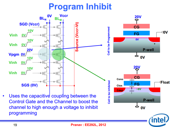
When programming a cell, a high voltage of around 20V is applied to the wordline of that cell. Of course, the problem is that you cannot apply voltage to just one cell because the whole wordline will be activated so in order to select a specific cell, the bitline of that cell is held at 0V. At the same time, the neighbouring bitlines are charged to about 6V because this increases the capacitance between the bitline and floating gate, which is turn negates enough of the capacitance between the control and floating gate that the electrons cannot tunnel through the tunnel oxide. This is crucial because if all the bitlines were held at 0V, then all the cells along that wordline would be programmed with the same value.
To erase a cell, a reverse operation is performed by keeping the wordline at 0V while issuing a ~20V voltage on the bitline, which makes the electrons flow in the opposite direction (i.e. from the floating gate back to the bitline/silicon).
The way NAND is programmed and erased is also its Achilles' Heel. Because such high voltage is needed, the insulators around the floating gate (i.e. ONO and tunnel oxide) wear out as the NAND goes through program and erase cycles. The wear out causes the insulators to lose their insulating characters, meaning that electrons may now be able to escape the floating or get trapped in tunnel oxide during a program or erase. This causes a change in the voltage state of the cell.
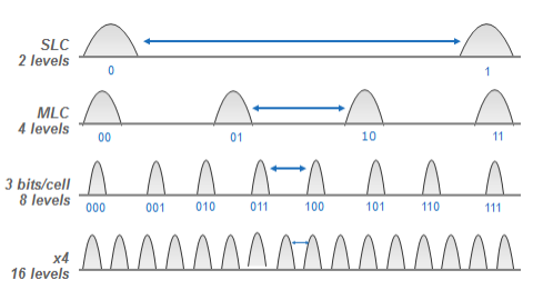
Remember, NAND uses the voltage states to define the bit value. If the charge in the floating gate is not what it is supposed to be, the cell may return an invalid value when read. With MLC and TLC this is even worse because the voltage states are much closer to each other, meaning that even minor changes in the voltage state may cause the voltage state to shift from its original position, which means the cell value will also change. Basically, MLC and TLC have less room for voltage state changes, which is why their endurance is lower because a cell that cannot hold its charge reliably is useless.
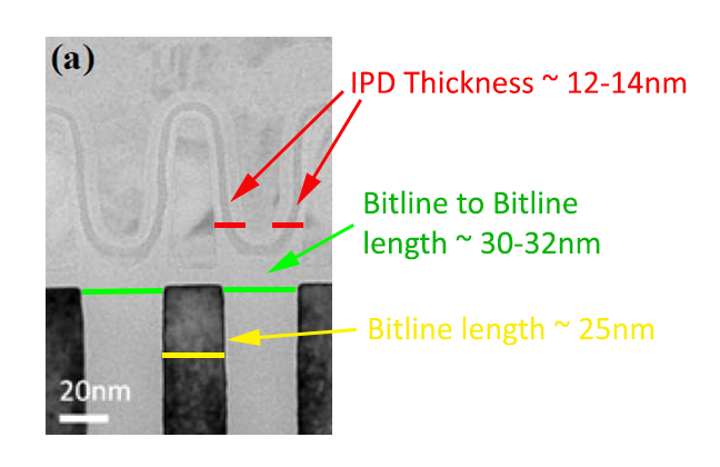
Now that we have covered the operation of NAND briefly, let's see what this has to do with scaling. Here is the same cross-section as above but with some dimensions attached.
That is what a cross-section of a single cell looks like. When NAND is scaled, all these dimensions get smaller, which means that individual cells are smaller as well as the distance between each cell. The cross-section above is of IMFT's 25nm NAND (hence the bitline length of 25nm), so it is not exactly current generation but unfortunately I do not have any newer photos. There is no general rule to how much the dimensions shrink because 16nm simply means that one of the lengths is 16nm while others may not shrink that much.
The scaling introduces a variety of issues but I will start with the cell size. As the cell size is shrunk, the size of the floating gate is also shrunk, which means that the floating gate is able to hold less and less electrons every time the process node gets smaller. To put this into perspective, Toshiba's and SanDisk's 15nm NAND is stores less than 20 electrons per NAND cell. With TLC, that is less than three electrons per voltage state, so there is certainly not much headroom for escaped electrons. In other words, the cell becomes more vulnerable to the IPD and tunnel oxide wear out because even the loss of one electron can be vital to the voltage state.
The second issue is the proximity of the cells. The key factor in NAND is the capacitance between the control and floating gate but as the cells move closer to each other through scaling, the neighboring cells will also introduce capacitive coupling. In simpler terms, the neighboring cells will interfere more as the distance between the cells shrinks. The obstacle is that the interference varies depending on the charge of the neighbouring cell, so there is no easy way to exclude the intereference. This in turn makes programming harder and more time consuming because a higher voltage will be needed to achieve the sufficient capacitance between the control and floating gate to make the eletrons tunnel through the oxide.
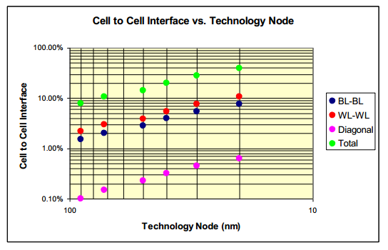
The graph above outlines historic rate of how cell to cell intereference increases through die shrinks. At 90nm, the interference was only around 8-9% but at 20nm it is a rather significant 40%. The interference means that 40% of the capacitive coupling comes from the other cells, making it very hard to control the gate you are trying to program or read. Fortunately as a result of some clever engineering (i.e. an airgap between the wordlines), the intererence is only about 25% at 25nm, which is much more managable than the 40% the historic rate would have given us.
The above can be fairly tough to digest, so let's do a simple analogy that everyone should be able to understand. Imagine that you have a bunch of speakers with each playing a different song. When these speakers are relatively large and far away from each other, it is easy to properly hear the song that the speaker closest to you is playing. Now, what happens if you bring the other speakers closer to the speaker you are listening? The other speakers will interfere and it becomes harder to tell your song apart from the others. If you turn down the volume or switch to smaller speakers with lower output volume, it becomes even harder to distinquish your song from the songs that the other songs that other speakers are playing. If you repeat this enough times, there will be a point when you are hearing your song as unclearly as the other songs.
The effect is essentially the same with NAND scaling. When the cells, or speakers in the analogy, move closer to each other, the amount of interference increases, making it harder to sense the cell or listen to the speaker. At the same time the size of the cell (or speakers) is shrunk, which further complicates the focus on one cell (or speaker).
That is NAND scaling and its issues in a nutshell. We have seen innovations such as airgaps between the wordlines to reduce cell-to-cell interference and a high K metal gate instead of a traditional ONO IPD to increase control gate to floating gate capacitance, but the limit has now been reached. However, like other semiconductors NAND must follow the Moore's Law in order to get more cost efficient. If you can no longer scale in the X and Y dimensions, what do you do? You hit the reset button and introduce the Z dimension.
3D NAND: How It Works
To understand how 3D NAND helps to keep Moore's Law in action, we first need to go in-depth with the structure. Before we begin, there are a couple of disclaimers I want to get out. First of all, every manufacturer has a different 3D NAND structure, so to avoid information overflow and confusion, I will only talk about Samsung's structure for now. When other manufacturers are ready with their 3D NAND products, I will provide a similar analysis of their structure. Secondly, there is not much detailed information about Samsung's 3D NAND, or V-NAND as they call it, so I am mostly basing my analysis on The Memory Guy's blog post (also known as Jim Handy, a respected semiconductor analyst).
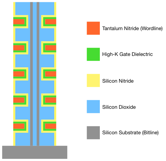
What you are seeing above is a 5-layer 3D NAND string based on Samsung's TCAT (Terabit Cell Array Transistor) structure. It consists of a total of ten cells and similar to 2D NAND each cell is capable of holding one, two or three bits of data depending on whether the NAND is SLC, MLC or TLC. Samsung's current (i.e. second) generation V-NAND has 32 layers, meaning that it is simply a taller tower but to keep the graph easily readable I decreased the number of layers to five.
There is one fundamental difference between Samsung's V-NAND. With 2D NAND, the charge was stored in a conductive floating gate but as you can see in the graph above, there is not one in Samsung's V-NAND. Instead Samsung uses a design called Charge Trap Flash (CTF), which means that the charge is stored in an insulator, which is silicon nitride in this case.
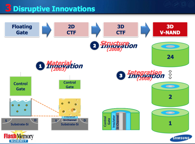
Some of you might remember this rather hilarious slide we used in our V-NAND announcement article and I now have an explanation as to why Samsung used cheese in in (yes, it indeed is cheese). A traditional floating gate works pretty much like a bucket of water. As long as there is not a hole in the bucket, the water stays there without an issue. However, if you get even a tiny hole in the bucket, all the water will sooner than later escape through that hole. It is the same with a floating gate because if there is a hole in the insulating material around it (Inter Poly Dielectric and tunnel oxide), all the electrons in the floating gate will escape through that as the floating gate is conductive and the electrons can move freely. As I mentioned on the previous page, this is exactly what happens when NAND is cycled and wears out because the stress caused by the programming operation causes the insulators to lose their insulating characteristics.
With Charge Trap Flash that does not happen because the electrons reside in an insulator. Samsung compared the bucket of water idea to cheese, meaning that if there is a hole the cheese will not just pour out from it like water would.
As a result, Charge Trap Flash increases endurance as it is not as vulnerable to wear out. I am also told that CTF does not require as high programming voltages as floating gates do (up to 20V), which reduces the stess on the insulators. I wonder if this is simply because the insulators do not have to be that thick anymore (a miminum of 7nm for tunnel oxide and 12nm for ONO) because the charge trap is not as dependent on the surrounding insulators as floating gate is. The reason why such a high voltage is needed for 2D NAND programming is the thickness of the tunnel oxide because otherwise the electrons cannot tunnel through (remember, the electrons are shot through an insulator). On the other hand, the tunnel oxide cannot be made any thinner than 7nm or otherwise data retention takes a massive hit (NAND is really an engineers dream, isn't it? Touch one thing and you break another).
Another interesting tidbit regarding Samsung’s V-NAND is the usage of a high-K dielectrics. IMFT did a similar switch when they moved to 20nm node but all the other manufacturers, as far as I know, have stayed with an inter poly dielectric (IPD) design. I went into detail about high-K dielectrics in our Crucial MX100 review but I will provide a quick summary here. Basically, a high-K dielectric is a material with a high dielectric constant, which is quite surprisingly known as K. The benefit of a high-K dielectric over a normal dielectric (like oxide-nitride-oxide i.e. ONO in NAND) is that it provides a higher capacitance between the word and bitlines. Similar to 2D NAND, the capacitance between the control gate and the floating gate, or charge trap in the case of V-NAND, is still the key factor for operation. The usage of high-K dielectrics gives Samsung a bit more headroom in terms of vertical scaling as layers can be stacked closer to each other and it also improves endurance as high-K dielectrics have less leakage compared to normal dielectrics.
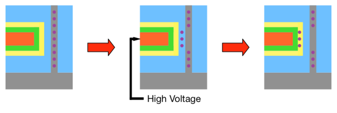
Otherwise the basics of V-NAND are very similar to 2D NAND. To program a cell, the bitline is grounded (i.e. held at 0V) while a high voltage is placed on the wordline. That makes the electrons that are floating in the bitline to tunnel through the silicon dioxide to the charge trap a.k.a. silicon nitride.
I made a very simple graph of V-NAND programming, which should help you to understand the process. The elements are the same as in the tower graph with the difference that it is just one layer and I cut the tower in half to fit it on the page. The purple balls are electrons.
Reading from V-NAND works exactly the same as with 2D NAND. The wordline of the cell-to-be-read is held at 0V while different voltages are applied on the bitline. Once the correct voltage is found, the cell will conduct and the sense amp will read the data depending on what the voltage was (the voltage determines the voltage state, i.e. what the value is).
3D NAND: Hitting The Reset Button on Scaling
Now that we understand how 3D NAND works, it is time to see what it is all about. As we now know, the problem with 2D NAND is the shrinking cell size and the proximity of the cells, which results in degraded reliability and endurance. Basically, 3D NAND must solve these two issues but it must also remain scalable to be economical. So how does it do that? This is where the third dimension comes into play.
The cost of a semiconductor is proportional to the die size. If you shrink the die, you effectively get more dies from a single wafer, resulting in a lower cost per die. Alternatively you can add more functionality (i.e. transistors) to each die. In the case of NAND, that means you can build a higher capacity die while keeping the die size the same, which gives more gigabits per wafer and thus reducing cost. If you cannot shrink the die, then you have just hit a dead-end because the cost will not scale. That is what has happened with 2D NAND because the shrinks on X and Y axes have run out of gas.
What 3D NAND does is add a Z-axis to the game. Because it stacks cells vertically, it is no longer as dependent on the X and Y axes since the die size can be reduced by adding more layers. As a result, Samsung's V-NAND takes a more relaxed position on the X and Y axes by going back to a 40nm process node, which increases the cell size and leaves more room between individual cells, eliminating the major issues 2D NAND has. The high amount of layers compensates for the much larger process node, resulting in a die that is the same size and capacity as the state of the art 2D NAND dies but without the caveats.
The above graph gives some guidance as to how big each cell in V-NAND really is. On the next page, I will go through the method of how cell size is really calculated and how V-NAND compares with Micron’s 16nm NAND but the above gives a good picture of the benefit that 3D NAND has. Obviously, when each cell is larger and the distance between individual cells is higher, there are more electrons to play with (i.e. more room for voltage state changes) and the cell to cell interference decreases substantially. Those two are the main reasons why V-NAND is capable of achieving up to ten times the endurance of 2D NAND.
Moreover, scaling in vertical dimension does not have the same limitations as scaling in the X and Y axes do. Because the cost of a semiconductor is still mostly determined by the die area and not by the height, there is no need to cram cells very close to each other. As a result, there is very little interference between the cells even in the vertical direction. Also, the usage of high-K dielectrics means that the control gate does not have to wrap around the charge trap. The result is that there is a hefty barrier of silicon dioxide (which is an insulator) between each cell, which is far more insulating than the rather thin ONO layer in 2D NAND. Unfortunately, I do not know what is the exact distance between each cell in the vertical dimension but I think it is safe to assume that it is noticeably more than the ~20nm in 2D NAND since there is no need for aggressive vertical scaling.
As for how far Samsung believes their V-NAND can scale, their roadmap shows a 1Tbit die planned for 2017. That is very aggressive because it essentially implies that the die capacity will double every year (256Gbit next year, 512Gbit in 2016 and finally 1Tbit in 2017). The most interesting part is that Samsung is confident that they can do this simply by increasing the layer count, meaning that the process node will stay at 40nm.
3D NAND in Numbers: Is it Economical?
As with all new semiconductor technologies, the one big question is whether it is economical. There are a ton of memory technologies that have better characteristics than 2D NAND (MRAM and ReRAM to name a couple) but none of them is currently scalable enough to challenge NAND in cost. IMFT's 16nm node is the smallest node shipping in volume, so let's compare Samsung's second generation V-NAND to that to see how it stacks up.
I am basing my analysis on Andrew Walker's blog post from 3DInCites. He is a respected analyst in 3D technologies and his blog post is based on Samsung's and Micron's presentations at the 2014 International Solid-State Circuits Conference, so the data should be as accurate as it can be.
Update 7/8: I was able to find some more accurate data regarding the die size, so I've updated this section with the new data.
| Samsung 2nd Gen V-NAND | Micron 16nm NAND | |
| Process Node | 40nm | 16nm |
| # of Layers | 32 | - |
| Die Capacity | 86Gbit | 128Gbit |
| Die Size | 95.4mm2 | 173mm2 |
| Cell Size | 40,300nm2 | 1,312nm2 |
The only downside of Walker's data is that it only covers Samsung's first generation V-NAND, which was a 24-layer design with a die size of 133mm2 and capacity of 128Gbit. Fortunately, the second generation V-NAND is using the same 40nm node, so the only substantial difference between the first and second generation is the number of layers. The 86Gbit die capacity is certainly a bit odd but it actually makes sense as it is simply the first generation die cut in half with the added layers [(128Gbit / 2) * (32 / 24)]. As such, it is relatively safe to assume that the other variables (cell size etc.) are the same as with the first generation and that is what the table above is based on.
Update 7/8: Actually, the peripheral circuitry does not scale with the memory array, meaning that the die size is actually quite a bit larger than I originally thought.
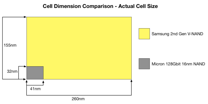
Before we go deeper with the density analysis, I want to explain how cell size is calculated. As you can see, the figures are way too big to make any sense if you just look at the 40nm and 16nm figures because no matter how you try to multiply them, the results do not make sense.
Oftentimes when cell size is discussed, it is only the actual size of the cell that is taken into account, which leaves the distance between cells out of the conclusion. However, the so called empty parts (they are not really empty as you saw in the X-ray a couple of pages back) take a part of the die area similar to the cells, meaning that they cannot be excluded. The appropriate way to measure cell size is from the inner corner of a cell to the outer corners of neighbouring cells in both X and Y axes. This is demonstrated by the black square on the above graph.
With the proper measurements, this is how V-NAND compares to 16nm NAND when just looking at cell size alone (i.e. excluding how the layers impact density). Doesn't look too good, huh?
If you are wondering where the 16nm comes from, it is mostly just marketing. 16nm refers to the smallest length (or resolution as it is often called) in the die, meaning that it is the finest line that can be printed. In the case of NAND, that can either be the wordline or bitline, or the distance between them. With Micron's 16nm NAND, that is likely the length of the wordline and the distance between two wordlines as the two are 32nm when combined (i.e. 16nm each).
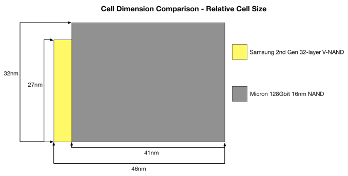
The actual cell size did not make justice to V-NAND because the whole idea behind the move to 3D NAND is to increase the cell size and distances between cells to get rid of the issues 2D NAND has. In the graph above, I took the amount of layers into account because you essentially need 32 2D NAND cells to achieve the same density as with 32-layer V-NAND and the game totally changes.
The math behind that graph is just a couple of simple arithmetic equations. The actual cell area is 40,300 (155nm*260nm), meaning that the relative cell area is simply the actual cell area divided by the number of layers. That gives us 1,259nm2(40,300nm2 / 32). To get the relative dimensions, the actual dimensions are divided by the square root of the number of layers (e.g. 155nm / √32 = 27nm).
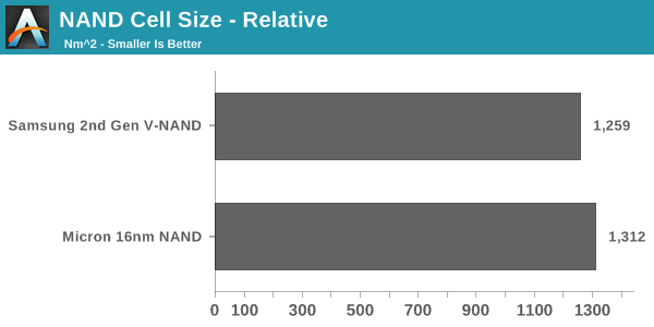
In the end, the relative cell size turns out to be smaller than Micron's 16nm NAND. The difference is not huge (~4%) but when the performance, power consumption and endurance advantages are taken into account, V-NAND is a clear winner.
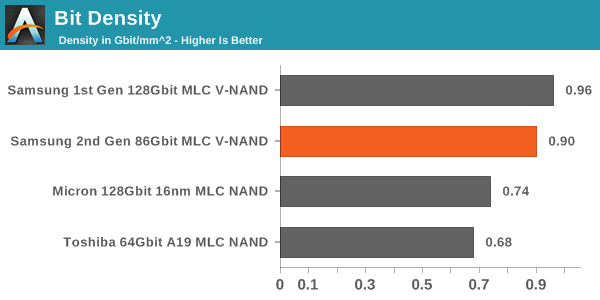
Another way to look at cost efficiency is the bit density. While cell size is a good measure, it does not take peripheral circuitry and ECC/spare bytes into account, which take a part of the die as well. Bit density is simply die capacity divided by die size and it gives us a number for quick and easy comparison.
In this comparison, V-NAND is the leader without any doubts. The bit density is as much as 73% higher, resulting in a much more cost efficient design. The reason why the difference between cell size and bit density is so large is that 2D NAND requires a lot more die area for ECC bytes because it is more error prone. With V-NAND there is less ECC needed thanks to its higher reliability. In addition, Micron's peripheral circuitry design is relatively die consuming, so I wonder how Toshiba's/SanDisk's 15nm stacks up with V-NAND as they are claiming to have a more efficient peripheral circuitry design.
Update 7/8: V-NAND is still denser than the latest 2D NAND nodes but the difference is not overwhelming.
All in all, there is a lot more than just cell area and bit density when it comes to cost efficiency. Yield and equipment cost are two major factors, which are both better for 2D NAND as it is a well known technology and some of the machinery can be reused when moving from one node to another.
RAPID 2.0: Support For More RAM & Updated Caching Algorithm
When the 840 EVO launched a year ago, Samsung introduced a new feature called RAPID (Real-time Accelerated Processing of I/O Data). The idea behind RAPID is very simple: it uses the excess DRAM in your system to cache IOs, thus accelerating storage performance. Modern computers tend to have quite a bit of DRAM that is not always used by the system, so RAPID turns a portion of that into a DRAM cache.
With the 850 Pro, Samsung is introducing Magician 4.4 along with an updated version of RAPID. The 1.0 version of RAPID supported up to 1GB of DRAM (or up to 25% if you had less than 4GB of RAM) but the 2.0 version increases the RAM allocation to up to 4GB if you have 16GB of RAM or more. There is still the same 25% limit, meaning that RAPID will not use 4GB of your RAM if you only have 8GB installed in your system.
I highly recommend that you read the RAPID page of our 840 EVO review because Anand explained the architecture and behavior of RAPID in detail, so I will keep the fundamentals short and focus on what has changed.
In addition to increasing the RAM allocation, Samsung has also improved the caching algorithms. Unfortunately, I was not able to get any details before the launch but I am guessing that the new version includes better optimization for file types and IO sizes that get the biggest benefit from caching. Remember, while RAPID works at the block level, the software also looks at the file types to determine what files and IO blocks should be prioritized. The increased RAM allocation also needs an optimized set of caching algorithms because with a 4GB cache RAPID is able to cache more data at a time, which means it can relax the filetype and block size restrictions (i.e. it can also cache larger files/IOs).
To test how the new version of RAPID performs, I put it through our Storage Benches as well as PCMark 8’s storage test. Our testbed is equipped with 32GB of RAM, so we should be able to get the full benefit of RAPID 2.0.
| Samsung SSD 850 Pro 256GB | ||||
| ATSB - Heavy 2011 Workload (Avg Data Rate) | ATSB - Heavy 2011 Workload (Avg Service Time) | ATSB - Light 2011 Workload (Avg Data Rate) | ATSB - Light 2011 Workload (Avg Service Time) | |
| RAPID Disabled | 310.8MB/s | 676.7ms | 366.6MB/s | 302.5ms |
| RAPID Enabled | 549.1MB/s | 143.4ms | 664.4MB/s | 134.6ms |
The performance increase in our Storage Benches is pretty outstanding. In both the Heavy and Light suites the increase in throughput is around 80%, making the 850 Pro even faster than the Samsung XP941 PCIe SSD.
| Samsung SSD 850 Pro 1TB | ||||
| PCMark 8 - Storage Score | PCMark 8 - Storage Bandwidth | |||
| RAPID Disabled | 4998 | 298.6MB/s | ||
| RAPID Enabled | 5046 | 472.8MB/s | ||
PCMark 8, on the other hand, tells a different story. As you can see, the bandwidth is again much faster, about 60%, but the storage score is only a mere 1% higher.
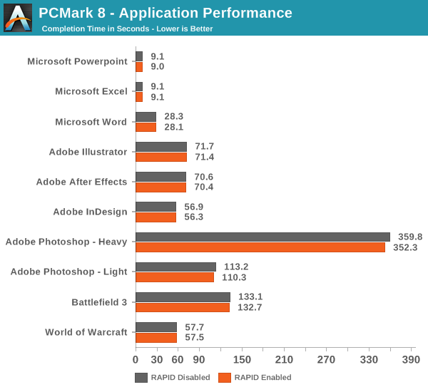
PCMark 8 also records the completion time of each task in the storage suite, which gives us an explanation as to why the storage scores are about equal. The fundamental issue is that today’s applications are still designed with hard drives in mind, meaning that they cannot utilize the full potential of SSDs. Even though the throughput is much higher with RAPID, the application performance is not because the software has been designed to wait several milliseconds for each IO to complete, so it does not know what to do when the response time is suddenly in the magnitude of a millisecond or two. That is why most applications load the necessary data to RAM when launched and only access storage when it is a must as back in the hard drive days, you wanted to avoid touching the hard drive as much as possible.
It will be interesting to see what the industry does with the software stack over the next few years. In the enterprise, we have seen several OEMs release their own APIs (like SanDisk’s ZetaScale) so companies can optimise their server software infrastructure for SSDs and take the full advantage of NAND. I do not believe that a similar approach works for the client market as ultimately everything is on the hands of Microsoft.
I also tried running the 2013 suite, a.k.a. The Destroyer, but for some reason RAPID did not like that and the system BSODed midway through the test. I am thinking that this is because our Storage Benches are ran without a partition, whereas RAPID also works at the file system level in the sense that it takes hints of what files should be cached. Due to that, it may be as simple as that under a high queue depth workload (like the ATSB2013), RAPID does not know what IOs to cache because there is no filesystem to guide it. I faced the same BSOD issue immediately when I fired up our IO consistency test (also ran without a partition), but when I tested with a similar 4KB random write workload using the new Iometer (which supports filesystem testing), there was absolutely no issue. This further suggests that the issue lies in our tests instead of the RAPID software itself as end-users will always run the drive with a partition anyway.
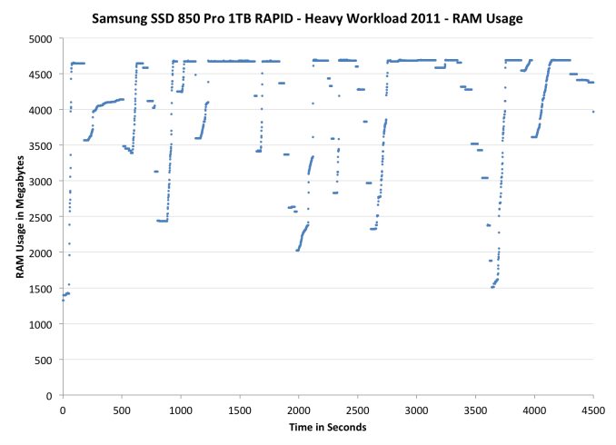
As Anand mentioned in the 840 EVO review, it is possible to monitor RAPID’s RAM usage by looking at the non-paged RAM pool. Instead of just looking at the resource monitor, I decided to take the monitoring one step further by recording the RAM usage over time with Windows’ Performance Monitor while running the 2011 Heavy workload. RAPID seems to behave fairly aggressively when it comes to RAM caching as the RAM usage increases to ~4.7GB almost immediately after firing up the test and stays there almost throughout the test. There are some drops, although I am not sure what is causing them. The idle times are limited to a maximum of 25 seconds when running the trace, so some drops could be caused by that. I need to do run some additional test and monitor the IOs to see if it is just the idle times of whether RAPID is excluding certain types of IOs.
I also ran ATTO to see how the updated RAPID responses to different transfer sizes. It looks like read performance scales quite linearly until hitting the IO size of 256KB. ATTO stores its performance values in 32-bit integers and with RAPID enabled performance exceeds the size of the result variable, thus wrapping around back to 0.
With writes, RAPID continues to cache fluently until hitting 1MB, which is when it starts to cache less aggressively.
Performance Consistency
Performance consistency tells us a lot about the architecture of these SSDs and how they handle internal defragmentation. The reason we don’t have consistent IO latency with SSD is because inevitably all controllers have to do some amount of defragmentation or garbage collection in order to continue operating at high speeds. When and how an SSD decides to run its defrag or cleanup routines directly impacts the user experience as inconsistent performance results in application slowdowns.
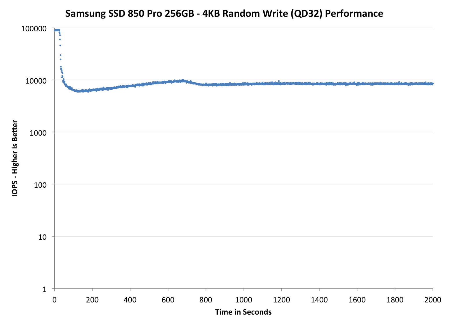
To test IO consistency, we fill a secure erased SSD with sequential data to ensure that all user accessible LBAs have data associated with them. Next we kick off a 4KB random write workload across all LBAs at a queue depth of 32 using incompressible data. The test is run for just over half an hour and we record instantaneous IOPS every second.
We are also testing drives with added over-provisioning by limiting the LBA range. This gives us a look into the drive’s behavior with varying levels of empty space, which is frankly a more realistic approach for client workloads.
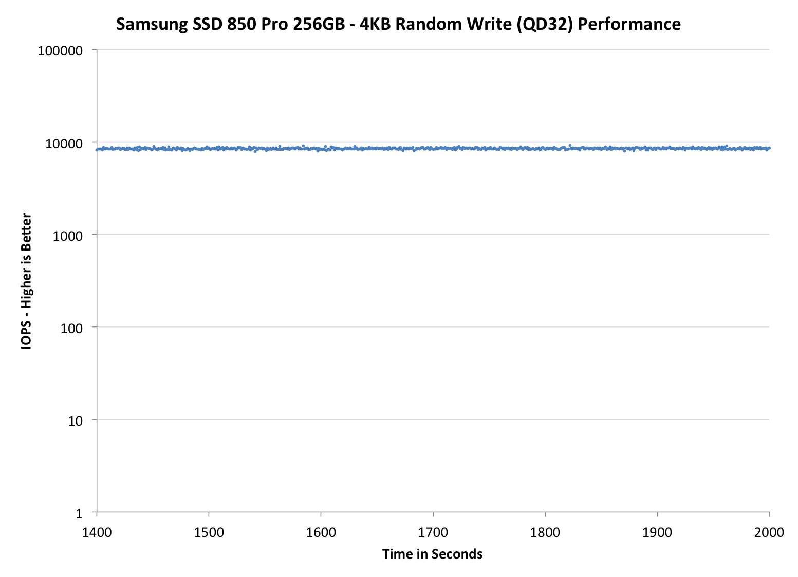
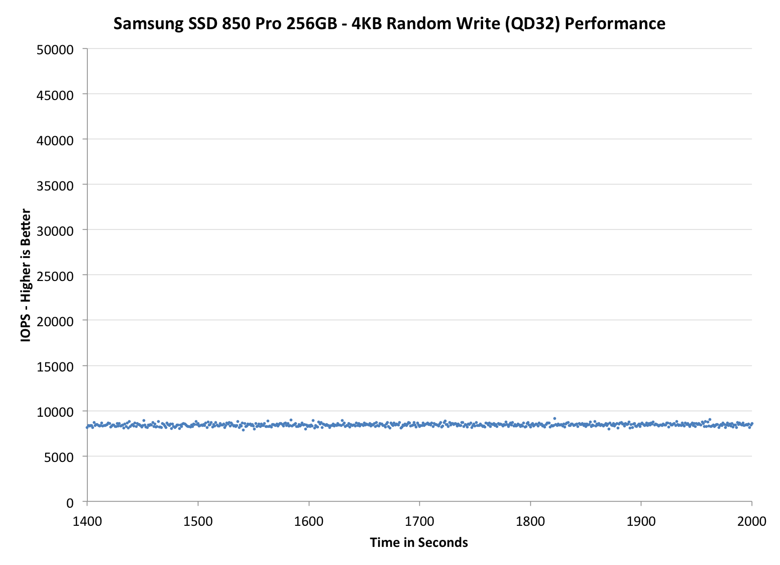
Each of the three graphs has its own purpose. The first one is of the whole duration of the test in log scale. The second and third one zoom into the beginning of steady-state operation (t=1400s) but on different scales: the second one uses log scale for easy comparison whereas the third one uses linear scale for better visualization of differences between drives. Click the buttons below each graph to switch the source data.
For more detailed description of the test and why performance consistency matters, read our original Intel SSD DC S3700 article.
 |
|||||||||
| Samsung SSD 850 Pro | Samsung SSD 840 Pro | SanDisk Extreme Pro | Intel SSD 730 | OCZ Vector 150 | |||||
| 7% Over-Provisioning | - | - | - | ||||||
| 12% Over-Provisioning | |||||||||
| 25% Over-Provisioning | |||||||||
Wow, this is awesome. Even with the default 7% over-provisioning, the 850 Pro is pushing almost as many IOPS as the Extreme Pro with its 12% over-provisioning. When the over-provisioning is increased to the same 12% level, the 850 Pro is a leader without a doubt. Only the Vector 150 can come close, although it is nowhere hear as constant as the IOPS is ranging between 10K and 30K, whereas the 850 Pro can maintain a steady line.
When compared with the 840 Pro, the upgrade is tremendous. IO consistency was always the weak point of the 840 Pro, so it is great to see that Samsung has paid a great effort to fix that in the 850 Pro. A part of the performance increase obviously comes from the usage of V-NAND because with shorter program and erase latencies, the steady-state performance increases as the garbage collection takes less time and there are more empty blocks available.
Some of you may wonder the odd capacities at 25% over-provisioning but the reason is that I noticed an error in the old ones. Basically, the old 25% numbers were in gibibytes (i.e. 1024^3 bytes) whereas the other capacities have always been in gigabytes (1000^3 bytes). I decided to unify the capacities and now they are all reported in gigabytes. The actual testing or over-provisioning levels have not changes -- it is simply a matter of how the capacities are represented.
 |
|||||||||
| Samsung SSD 850 Pro | Samsung SSD 840 Pro | SanDisk Extreme Pro | Intel SSD 730 | OCZ Vector 150 | |||||
| 7% Over-Provisioning | - | - | - | ||||||
| 12% Over-Provisioning | |||||||||
| 25% Over-Provisioning | |||||||||
 |
|||||||||
| Samsung SSD 850 Pro | Samsung SSD 840 Pro | SanDisk Extreme Pro | Intel SSD 730 | OCZ Vector 150 | |||||
| 7% Over-Provisioning | - | - | - | ||||||
| 12% Over-Provisioning | |||||||||
| 25% Over-Provisioning | |||||||||
AnandTech Storage Bench 2013
Our Storage Bench 2013 focuses on worst-case multitasking and IO consistency. Similar to our earlier Storage Benches, the test is still application trace based - we record all IO requests made to a test system and play them back on the drive we are testing and run statistical analysis on the drive's responses. There are 49.8 million IO operations in total with 1583.0GB of reads and 875.6GB of writes. I'm not including the full description of the test for better readability, so make sure to read our Storage Bench 2013 introduction for the full details.
| AnandTech Storage Bench 2013 - The Destroyer | ||
| Workload | Description | Applications Used |
| Photo Sync/Editing | Import images, edit, export | Adobe Photoshop CS6, Adobe Lightroom 4, Dropbox |
| Gaming | Download/install games, play games | Steam, Deus Ex, Skyrim, Starcraft 2, BioShock Infinite |
| Virtualization | Run/manage VM, use general apps inside VM | VirtualBox |
| General Productivity | Browse the web, manage local email, copy files, encrypt/decrypt files, backup system, download content, virus/malware scan | Chrome, IE10, Outlook, Windows 8, AxCrypt, uTorrent, AdAware |
| Video Playback | Copy and watch movies | Windows 8 |
| Application Development | Compile projects, check out code, download code samples | Visual Studio 2012 |
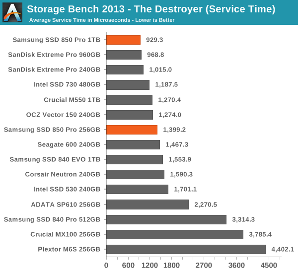
We are reporting two primary metrics with the Destroyer: average data rate in MB/s and average service time in microseconds. The former gives you an idea of the throughput of the drive during the time that it was running the test workload. This can be a very good indication of overall performance. What average data rate doesn't do a good job of is taking into account response time of very bursty (read: high queue depth) IO. By reporting average service time we heavily weigh latency for queued IOs. You'll note that this is a metric we have been reporting in our enterprise benchmarks for a while now. With the client tests maturing, the time was right for a little convergence.
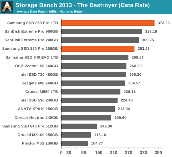
Thanks to the excellent IO consistency, the 850 Pro dominates our 2013 Storage Bench. At the 1TB capacity point, the 850 Pro is over 15% faster than any drive when looking at the average data rate. That is huge because the 850 Pro has less over-provisioning than most of today's high-end drives and the 2013 Storage Bench tends to reward drives that have more over-provisioning because it essentially pushes drives to steady-state. The 256GB model does not do as well as the 1TB one but it is still one of the fastest drives in its class. I wonder if the lesser amount of over-provisioning is the reason or perhaps the Extreme Pro is just so well optimized for mixed workloads.
AnandTech Storage Bench 2011
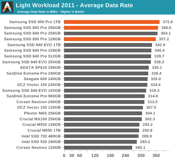
Back in 2011 (which seems like so long ago now!), we introduced our AnandTech Storage Bench, a suite of benchmarks that took traces of real OS/application usage and played them back in a repeatable manner. The MOASB, officially called AnandTech Storage Bench 2011 - Heavy Workload, mainly focuses on peak IO performance and basic garbage collection routines. There is a lot of downloading and application installing that happens during the course of this test. Our thinking was that it's during application installs, file copies, downloading and multitasking with all of this that you can really notice performance differences between drives. The full description of the Heavy test can be found here, while the Light workload details are here.
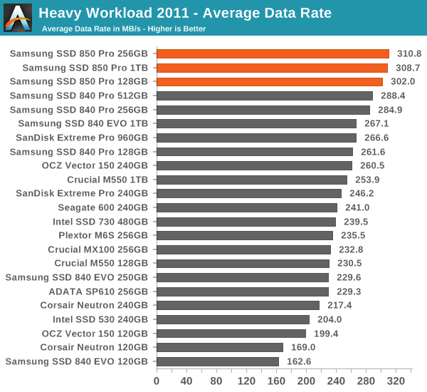
The dominance continues in our 2011 Storage Benches. The 840 Pro was already the fastest drive in both suites, so it does not come as a surprise that the 850 Pro takes the lead.
Random Read/Write Speed
The four corners of SSD performance are as follows: random read, random write, sequential read and sequential write speed. Random accesses are generally small in size, while sequential accesses tend to be larger and thus we have the four Iometer tests we use in all of our reviews.
Our first test writes 4KB in a completely random pattern over an 8GB space of the drive to simulate the sort of random access that you'd see on an OS drive (even this is more stressful than a normal desktop user would see). We perform three concurrent IOs and run the test for 3 minutes. The results reported are in average MB/s over the entire time.
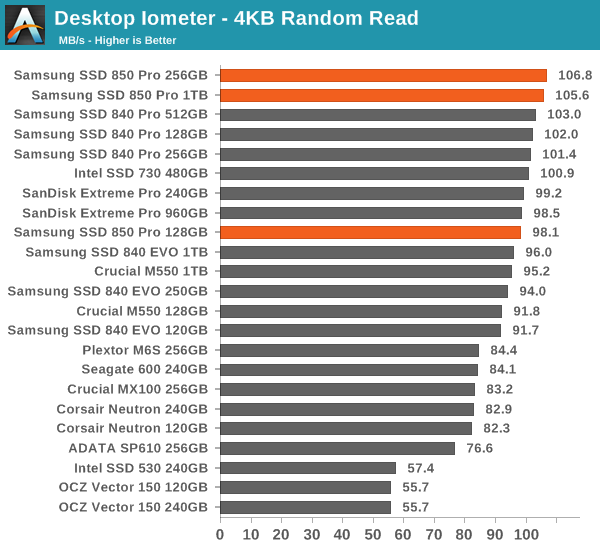
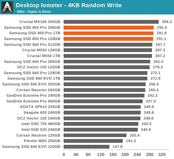
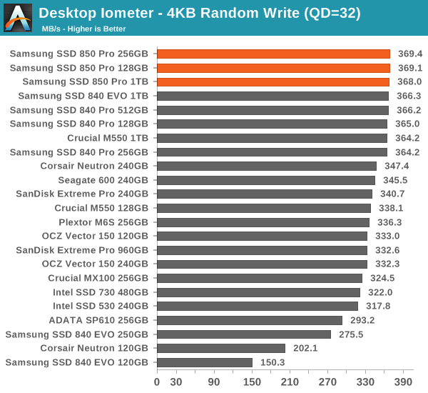
Random performance is also brilliant and the 850 Pro tops almost all of our benchmarks. It is no wonder why it is so fast in the Storage Benches.
Sequential Read/Write Speed
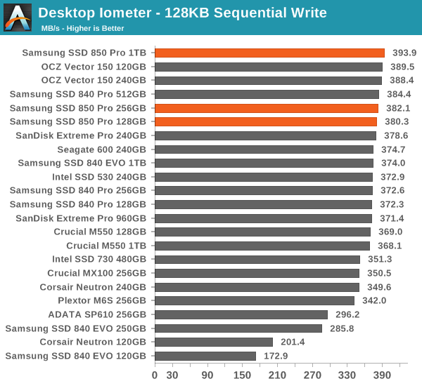
To measure sequential performance we run a 1 minute long 128KB sequential test over the entire span of the drive at a queue depth of 1. The results reported are in average MB/s over the entire test length.
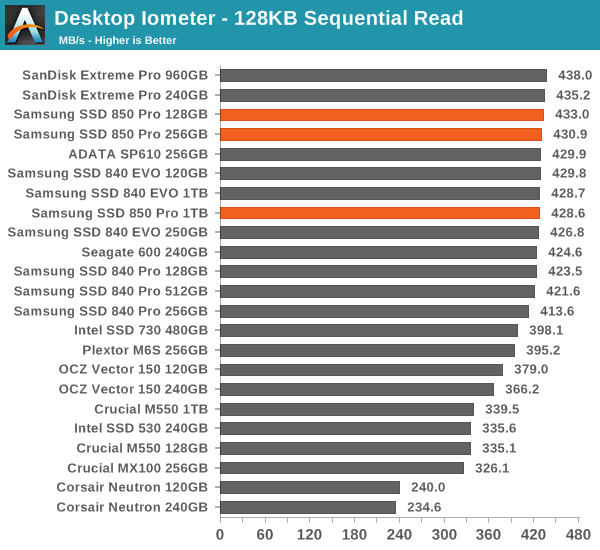
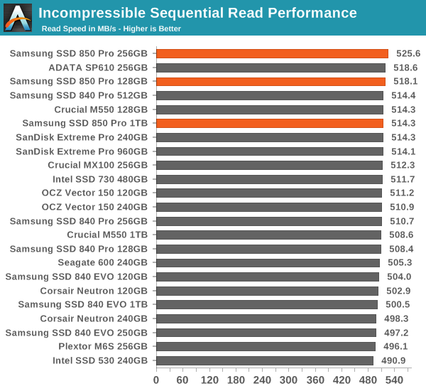
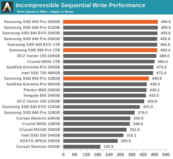
The same goes for sequential speeds. Of course, the differences are not substantial but nevertheless the 850 Pro is fast.
AS-SSD Incompressible Sequential Read/Write Performance
The AS-SSD sequential benchmark uses incompressible data for all of its transfers. The result is a pretty big reduction in sequential write speed on SandForce based controllers, but it doesn't impact most of the other controller much if at all.
Performance vs. Transfer Size
ATTO is a useful tool for quickly benchmarking performance across various transfer sizes. You can get the complete data set in Bench. To highlight the performance of each capacity, I decided to divide the ATTO graphs by each capacity, which should also make the graphs a bit more readable.
IO size scaling remain very similar to the 840 Pro and EVO. It is only at the 128GB capacity where the V-NAND provides a substantial advantage and the 850 Pro is almost as fast as the 120GB Intel SSD 525, which is a SandForce based drive, so its high performance is explained by ATTO's use of compressible data.
Power Consumption
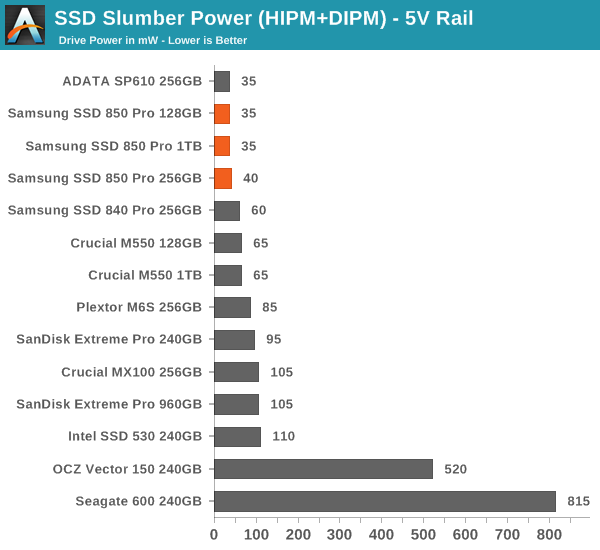
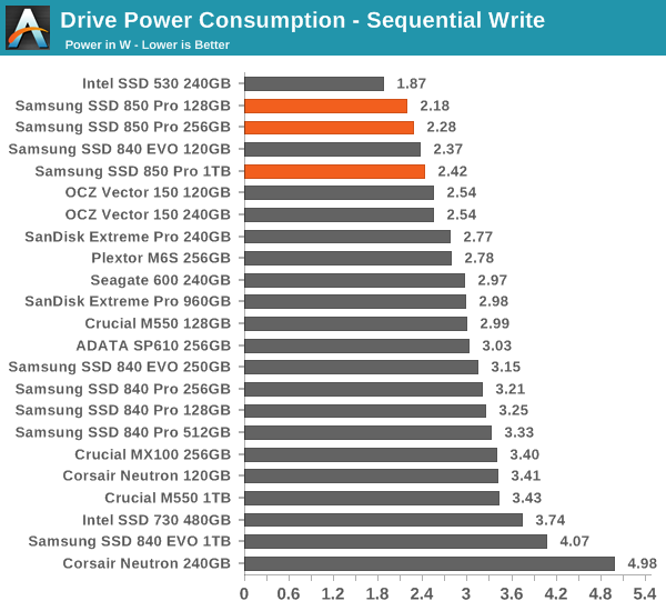
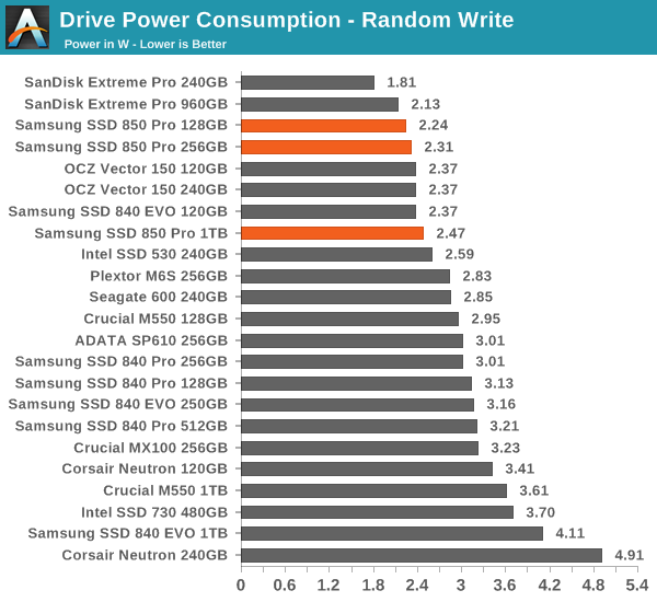
Samsung has always been pushing hard with power consumption and the 850 Pro is another proof of their efforts. Slumber power is down by a bit compared to the 840 Pro and generally speaking the 850 Pro is one of the most efficient drives. Even load power consumption stays at below 2.5W, which is superb given the performance of the 850 Pro.
Final Words
Samsung does not cease to amaze me with their SSDs as the 850 Pro just kills it in every aspect. The performance is there. The endurance is the best of the class. Heck, even Samsung's feature and software suites beat the competition by a mile. To be honest, there is not a single thing missing in the 850 Pro because regardless of the angle you look at the drive from, it it will still top the charts.
Samsung's heavy investment on NAND R&D and specifically 3D NAND is really paying off in the 850 Pro. Thanks to the more efficient structure of 3D NAND, Samsung has been able to improve all three main aspects of NAND i.e. performance, endurance and power consumption. It will be very hard for anyone to compete with the 850 Pro as the characteristics of V-NAND are superior compared to 2D NAND. The density is also very competitive against the smallest 2D NAND nodes, meaning that V-NAND should not carry a hefty premium over MLC.
| NewEgg Price Comparison (6/28/2014) | ||||
| 120/128GB | 240/256GB | 480/512GB | 960GB/1TB | |
| Samsung SSD 850 Pro (MSRP) | $130 | $200 | $400 | $700 |
| Samsung SSD 840 Pro | $120 | $190 | $401 | - |
| Samsung SSD 840 EVO | $80 | $140 | $240 | $420 |
| SanDisk Extreme Pro | - | $200 | $370 | $600 |
| SanDisk Extreme II | $80 | $150 | $260 | - |
| Crucial MX100 | $75 | $110 | $210 | - |
| Crucial M550 | $104 | $157 | $280 | $491 |
| Plextor M6S | $100 | $145 | $400 | - |
| Intel SSD 730 | - | $270 | $500 | - |
| Intel SSD 530 | $94 | $165 | $330 | - |
| OCZ Vector 150 | $115 | $190 | $370 | - |
Update: Samsung just provided us the updated MSRPs, which I have added to the table. The old MSRPs were $230 for 256GB, $430 for 512GB and $730 for the 1TB capacity. This certainly makes the 850 Pro more price competitive with the Extreme Pro, although the 1TB drive is still $100 more.
The MSRPs, on the other hand, are a bit of a letdown. I was hoping that Samsung would have priced the 850 Pro more aggressively because now they are asking anywhere between $30 and $130 more than what SanDisk is charging for the Extreme Pro. The 850 Pro is certainly a better drive in all areas but forking over up to $130 more for one can be difficult to justify. Of course, as with all MSRPs, they should be taken with a grain of salt and I certainly hope that the actual street prices end up being closer to the Extreme Pro ones the 850 Pro becomes available in the next few weeks.
If you are looking for a SATA 6Gbps drive and want the absolute best, the 850 Pro is your pick. It is without a doubt the best drive in the market as long as you are able to justify the price premium over other options.

