Sizing Up Servers: Intel's Skylake-SP Xeon versus AMD's EPYC 7000 - The Server CPU Battle of the Decade?
by Johan De Gelas & Ian Cutress on July 11, 2017 12:15 PM EST- Posted in
- CPUs
- AMD
- Intel
- Xeon
- Enterprise
- Skylake
- Zen
- Naples
- Skylake-SP
- EPYC
AMD's EPYC Server CPU
If you have read Ian's articles about Zen and EPYC in detail, you can skip this page. For those of you who need a refresher, let us quickly review what AMD is offering.
The basic building block of EPYC and Ryzen is the CPU Complex (CCX), which consists of 4 vastly improved "Zen" cores, connected to an L3-cache. In a full configuration each core technically has its own 2 MB of L3, but access to the other 6 MB is rather speedy. Within a CCX we measured 13 ns to access the first 2 MB, and 15 to 19 ns for the rest of the 8 MB L3-cache, a difference that's hardly noticeable in the grand scheme of things. The L3-cache acts as a mostly exclusive victim cache.
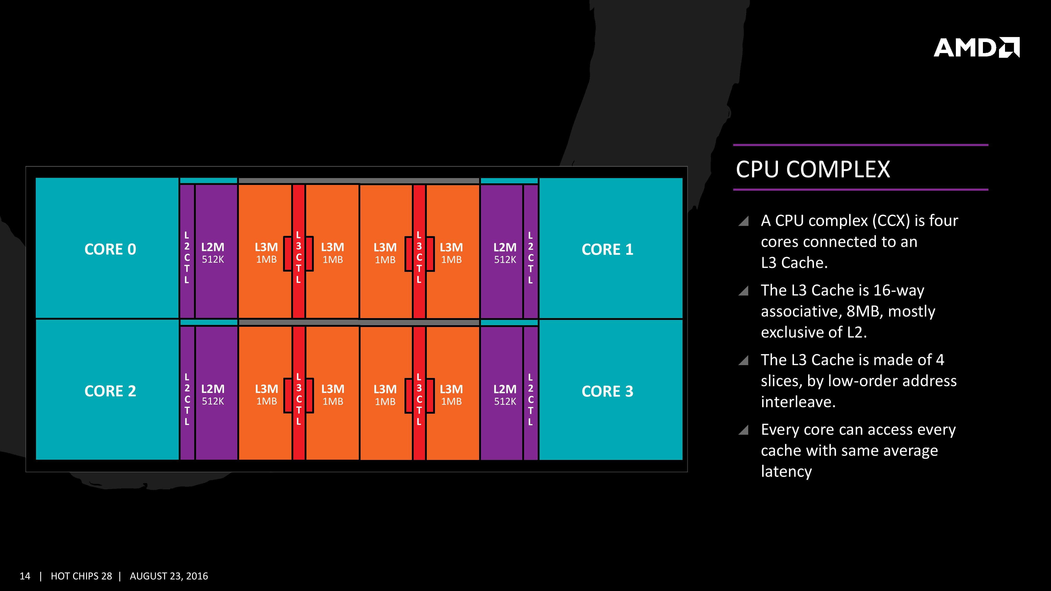
Two CCXes make up one Zeppelin die. A custom fabric – AMD's Infinity Fabric – ties together two CCXes, the two 8 MB L3-caches, 2 DDR4-channels, and the integrated PCIe lanes. That topology is not without some drawbacks though: it means that there are two separate 8 MB L3 caches instead of one single 16 MB LLC. This has all kinds of consequences. For example the prefetchers of each core make sure that data of the L3 is brought into the L1 when it is needed. Meanwhile each CCX has its own separate (not inside the L3, so no capacity hit) and dedicated SRAM snoop directory (keeping track of 7 possible states). In other words, the local L3-cache communicates very quickly with everything inside the same CCX, but every data exchange between two CCXes comes with a tangible latency penalty.
Moving further up the chain, the complete EPYC chip is a Multi Chip Module(MCM) containing 4 Zeppelin dies.
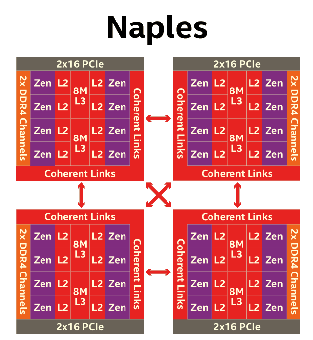
AMD made sure that each die is only one hop apart from the other, ensuring that the off-die latency is as low as reasonably possible.
Meanwhile scaling things up to their logical conclusion, we have 2P configurations. A dual socket EPYC setup is in fact a "virtual octal socket" NUMA system.

AMD gave this "virtual octal socket" topology ample bandwidth to communicate. The two physical sockets are connected by four bidirectional interconnects, each consisting of 16 PCIe lanes. Each of these interconnect links operates at +/- 38 GB/s (or 19 GB/s in each direction).
So basically, AMD's topology is ideal for applications with many independently working threads such as small VMs, HPC applications, and so on. It is less suited for applications that require a lot of data synchronization such as transactional databases. In the latter case, the extra latency of exchanging data between dies and even CCX is going to have an impact relative to a traditional monolithic design.


219 Comments
View All Comments
TheOriginalTyan - Tuesday, July 11, 2017 - link
Another nicely written article. This is going to be a very interesting next couple of months.coder543 - Tuesday, July 11, 2017 - link
I'm curious about the database benchmarks. It sounds like the database is tiny enough to fit into L3? That seems like a... poor benchmark. Real world databases are gigabytes _at best_, and AMD's higher DRAM bandwidth would likely play to their favor in that scenario. It would be interesting to see different sizes of transactional databases tested, as well as some NoSQL databases.psychobriggsy - Tuesday, July 11, 2017 - link
I wrote stuff about the active part of a larger database, but someone's put a terrible spam blocker on the comments system.Regardless, if you're buying 64C systems to run a DB on, you likely will have a dataset larger than L3, likely using a lot of the actual RAM in the system.
roybotnik - Wednesday, July 12, 2017 - link
Yea... we use about 120GB of RAM on the production DB that runs our primary user-facing app. The benchmark here is useless.haplo602 - Thursday, July 13, 2017 - link
I do hope they elaborate on the DB benchmarks a bit more or do a separate article on it. Since this is a CPU article, I can see the point of using a small DB to fit into the cache, however that is useless as an actual DB test. It's more an int/IO test.I'd love to see a larger DB tested that can fit into the DRAM but is larger than available caches (32GB maybe ?).
ddriver - Tuesday, July 11, 2017 - link
We don't care about real world workloads here. We care about making intel look good. Well... at this point it is pretty much damage control. So let's lie to people that intel is at least better in one thing.Let me guess, the databse size was carefully chosen to NOT fit in a ryzen module's cache, but small enough to fit in intel's monolithic die cache?
Brought to you by the self proclaimed "Most Trusted in Tech Since 1997" LOL
Ian Cutress - Tuesday, July 11, 2017 - link
I'm getting tweets saying this is a severely pro AMD piece. You are saying it's anti-AMD. ¯\_(ツ)_/¯ddriver - Tuesday, July 11, 2017 - link
Well, it is hard to please intel fanboys regardless of how much bias you give intel, considering the numbers.I did not see you deny my guess on the database size, so presumably it is correct then?
ddriver - Tuesday, July 11, 2017 - link
In the multicore 464.h264ref test we have 2670 vs 2680 for the xeon and epyc respectively. Considering that the epyc score is mathematically higher, howdoes it yield a negative zero?Granted, the difference is a mere 0.3% advantage for epyc, but it is still a positive number.
Headley - Friday, July 14, 2017 - link
I thought the exact same thing