5nm

Taiwan Semiconductor Manufacturing Co. this week said its revenue for the second quarter 2024 reached $20.82 billion, making it the company's best quarter (at least in dollars) to date. TSMC's high-performance computing (HPC) platform revenue share exceeded 52% for the first time in many years due to demand for AI processors and rebound of the PC market. TSMC earned $20.82 billion USD in revenue for the second quarter of 2024, a 32.8% year-over-year increase and a 10.3% increase from the previous quarter. Perhaps more remarkable, $20.82 billion is a higher result than the company posted Q3 2022 ($20.23 billion), the foundry's best quarter to date. Otherwise, in terms of profitability, TSMC booked $7.59 billion in net income for the quarter, for a gross margin of...

Huawei Announces Mate 40 Series: Powered by 15.3bn Transistors 5nm Kirin 9000
Today Huawei took the stage to unveil the new Mate 40 series of devices. In the form of the Mate 40, Mate 40 Pro and the Mate 40 Pro+...
107 by Andrei Frumusanu on 10/22/2020
Apple Announces 5nm A14 SoC - Meagre Upgrades, Or Just Less Power Hungry?
Amongst the new iPad and Watch devices released today, Apple made news in releasing the new A14 SoC chip. Apple’s newest generation silicon design is noteworthy in that is...
127 by Andrei Frumusanu on 9/15/2020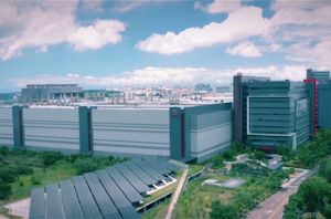
TSMC Expects 5nm to be 11% of 2020 Wafer Production (sub 16nm)
One of the measures of how quickly a new process node gains traction is by comparing how many wafers are in production, especially as that new process node goes...
13 by Dr. Ian Cutress on 8/25/2020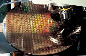
TSMC Details 3nm Process Technology: Full Node Scaling for 2H22 Volume Production
At TSMC’s annual Technology Symposium, the Taiwanese semiconductor manufacturer detailed characteristics of its future 3nm process node as well as laying out a roadmap for 5nm successors in the...
58 by Andrei Frumusanu on 8/24/2020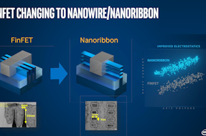
Intel to use Nanowire/Nanoribbon Transistors in Volume ‘in Five Years’
This year, at the international VLSI conference, Intel’s CTO Mike Mayberry gave one of the plenary presentations, which this year was titled ‘The Future of Compute’. Within the presentation...
14 by Dr. Ian Cutress on 6/22/2020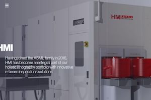
ASML’s First Multi-Beam Inspection Tool for 5nm
ASML has announced it has made a significant development in its multi-beam inspectional tool line. The new eScan1000 moves a single beam scanning process into a nine-beam scanning process...
19 by Dr. Ian Cutress on 6/1/2020
TSMC To Build 5nm Fab In Arizona, Set To Come Online In 2024
In a big shift to their manufacturing operations – and a big political win domestically – TSMC has announced that the company will be building a new, high-end fab...
100 by Ryan Smith on 5/15/2020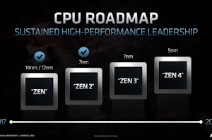
Updated AMD Ryzen and EPYC CPU Roadmaps March 2020: Milan, Genoa, and Vermeer
Everyone is interested in roadmaps – they give us a sense of an idea of what is coming in the future, and for the investors, it gives a level...
60 by Dr. Ian Cutress on 3/5/2020
TSMC & Broadcom Develop 1,700 mm2 CoWoS Interposer: 2X Larger Than Reticles
With transistor shrinks slowing and demand for HPC gear growing, as of late there has been an increased interest in chip solutions larger than the reticle size of a...
18 by Anton Shilov on 3/4/2020
Intel CFO: Our 10nm Will Be Less Profitable than 22nm [Morgan Stanley Transcription]
This week at Morgan Stanley’s Analyst Conference, Intel’s CFO, George Davis, sat down to discuss the future of where Intel’s profitability lies. No stranger to the odd comments relating...
92 by Dr. Ian Cutress on 3/4/2020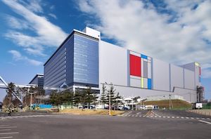
Samsung Starts Mass Production at V1: A Dedicated EUV Fab for 7nm, 6nm, 5nm, 4nm, 3nm Nodes
Samsung Foundry has started mass production of chips using its 6LPP and 7LPP manufacturing processes at its new V1 fab. The new facility employs one of the industry’s first...
30 by Anton Shilov on 2/20/2020
TSMC Boosts CapEx by $1 Billion, Expects N5 Node to Be Major Success
TSMC is on track to begin high-volume production of chips using its 5 nm technology in the coming months, the company said in its conference call last week. While...
40 by Anton Shilov on 1/22/2020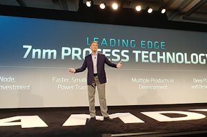
An Interview with AMD’s CTO Mark Papermaster: ‘There’s More Room At The Top’
On the back of a very busy 2019, AMD is gaining market share and is now a performance leader in a lot of CPU segments. The company has executed...
68 by Dr. Ian Cutress on 12/30/2019
Early TSMC 5nm Test Chip Yields 80%, HVM Coming in H1 2020
Today at the IEEE IEDM Conference, TSMC is presenting a paper giving an overview of the initial results it has achieved on its 5nm process. This process is going...
64 by Dr. Ian Cutress on 12/11/2019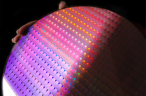
Intel’s Manufacturing Roadmap from 2019 to 2029: Back Porting, 7nm, 5nm, 3nm, 2nm, and 1.4 nm
One of the interesting disclosures here at the IEEE International Electron Devices Meeting (IEDM) has been around new and upcoming process node technologies. Almost every session so far this...
138 by Dr. Ian Cutress on 12/11/2019
TSMC: 5nm on Track for Q2 2020 HVM, Will Ramp Faster Than 7nm
TSMC’s 5 nm (N5) manufacturing technology is projected to provide significant benefits when it comes to performance, power, and area scaling, which is why the contract maker of semiconductors...
27 by Anton Shilov on 10/23/2019
TSMC Radically Boosts CapEx to Expand Production Capacities, To Reach $14B For 2019
Forecasting strong demand for its 5 nm and 7 nm class process technologies in the coming years, TSMC has announced that it's increasing its capital expenditure for 2019 by...
18 by Anton Shilov on 10/18/2019
New Tools & IP Accelerate Development of 5nm Arm ‘Hercules’ SoCs
Arm, Synopsys, and Samsung Foundry have developed a set of optimized tools and IP that will enable chip designers to build next-generation SoCs based on Arm’s Hercules processor cores...
9 by Anton Shilov on 10/10/2019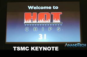
Hot Chips 31 Keynote Day 2: Dr. Phillip Wong, VP Research at TSMC (1:45pm PT)
The keynote for the second day is from TSMC, with Dr. Phillip Wong taking the stage to talk about the latest developments in TSMC's research and portfolio. The talk...
12 by Dr. Ian Cutress on 8/20/2019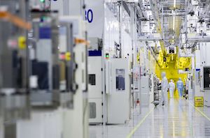
Samsung’s Aggressive EUV Plans: 6nm Production in H2, 5nm & 4nm On Track
Samsung Foundry formally started to produce chips using its 7LPP (7 nm low power plus) fabrication process last October and has not slowdown development of its manufacturing technologies since...
42 by Anton Shilov on 7/31/2019


