Intel Announces Atom E3900 Series - Goldmont for the Internet of Things & More
by Ryan Smith on October 25, 2016 9:00 AM EST
Kicking off a busy day for the Internet of Things market, Intel this morning is announcing the Atom E3900 series. Based upon the company’s latest generation Goldmont Atom CPU core, the E3900 series will be Intel’s most serious and dedicated project yet for the IoT market.
We’ve talked about Intel’s IoT efforts off and on over the past couple of years. Having largely missed the boat on mobile, the company decided it wouldn’t miss IoT as well, and as a result they’ve been making significant investments into the IoT market, treating it as a fourth pillar of their business. Their efforts have not gone unrewarded, as IoT revenue has continued to quickly grow over the years, and as of Q3’16, IoT is now Intel’s third largest business by revenue, ahead of non-volatile memory and behind only client and data center revenue. Furthermore with 19% year-over-year growth, IoT still looks like a growing market for the company.
Overall the company offers a number of IoT products, ranging from the tiny Curie to the relatively powerful Atom E-series. However to date, the company has never built a dedicated, high-end IoT die. The Atom E3800 series were Bay Trail, and the recently announced Joule devices use Broxton, Intel’s canceled-for-mobile Atom SoC. However today that will be changing, as the launch of the Atom E3900 series brings with it Intel’s first custom silicon targeting the roughly 6W to 12W market of more powerful IoT devices.
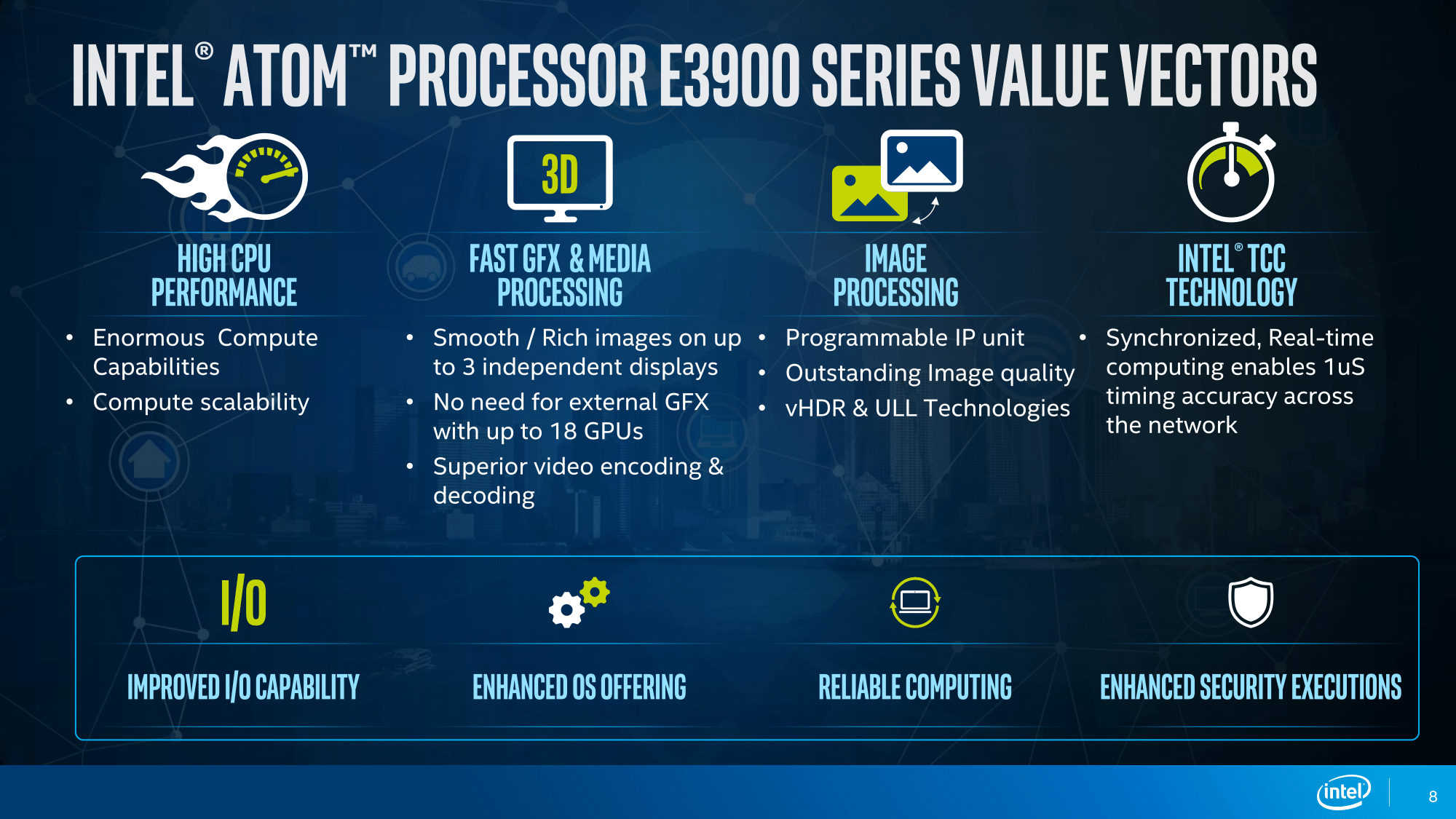
So what does an IoT-centric Atom look like? By and large, it’s Broxton and more. At its core we’re looking at 2 or 4 Goldmont CPU cores, paired with 12 or 18 EU configurations of Intel’s Gen9 iGPU. However this is where the similarities stop. Once we get past the CPU and GPU, Intel has added new features specifically for IoT in some areas, and in other areas they’ve gone and reworked the design entirely to meet specific physical and technical needs of the IoT market.
The big changes here are focused on security, determinism, and networking. Security is self-evident: Intel’s customers need to be able to build devices that will go out into the field and be hardened against attackers. Bits and pieces of this are inerieted from Intel’s existing Trusted Execution Technology, while other pieces, such as boot time measuring, are new. The latter is particularly interesting, as Intel is measuring the boot time of a system as a canary for if it’s been compromised. If the boot time suddenly and unexpectedly changes, then there’s a good chance the firmware and/or OS has been replaced.
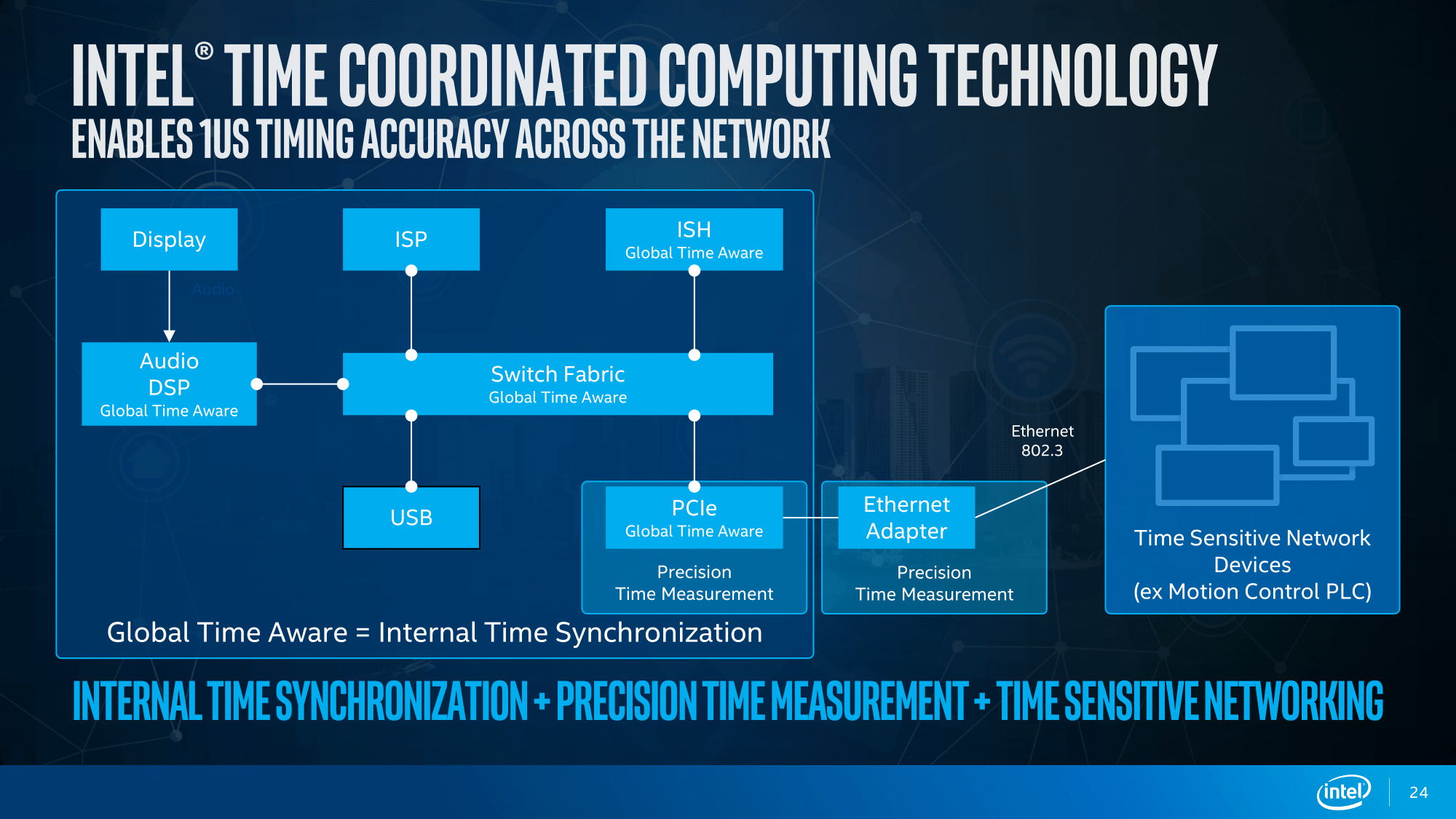
Meanwhile also new to the E3900 series is what Intel is calling their Time Coordinated Computing Technology. This high precision timing mechanism is to allow multiple Atom E3900s to be tightly synchronized, down to 1 microsecond. We’re told that this feature is of particular interest to Intel’s manufacturing partners, as a means to improve accuracy and synchronization between devices on a manufacturing line.

Finally, a bit more nebulous, the E3900 die also includes some changes specifically to improve determinism. What Intel is pitching here isn’t hard determinism, but a higher level of determinism for devices that need better guarantees about how soon an action will be completed. Apparently a big part of implementing this is at the cache level, with Intel noting that polling loops in particular were greatly impacted by this change.
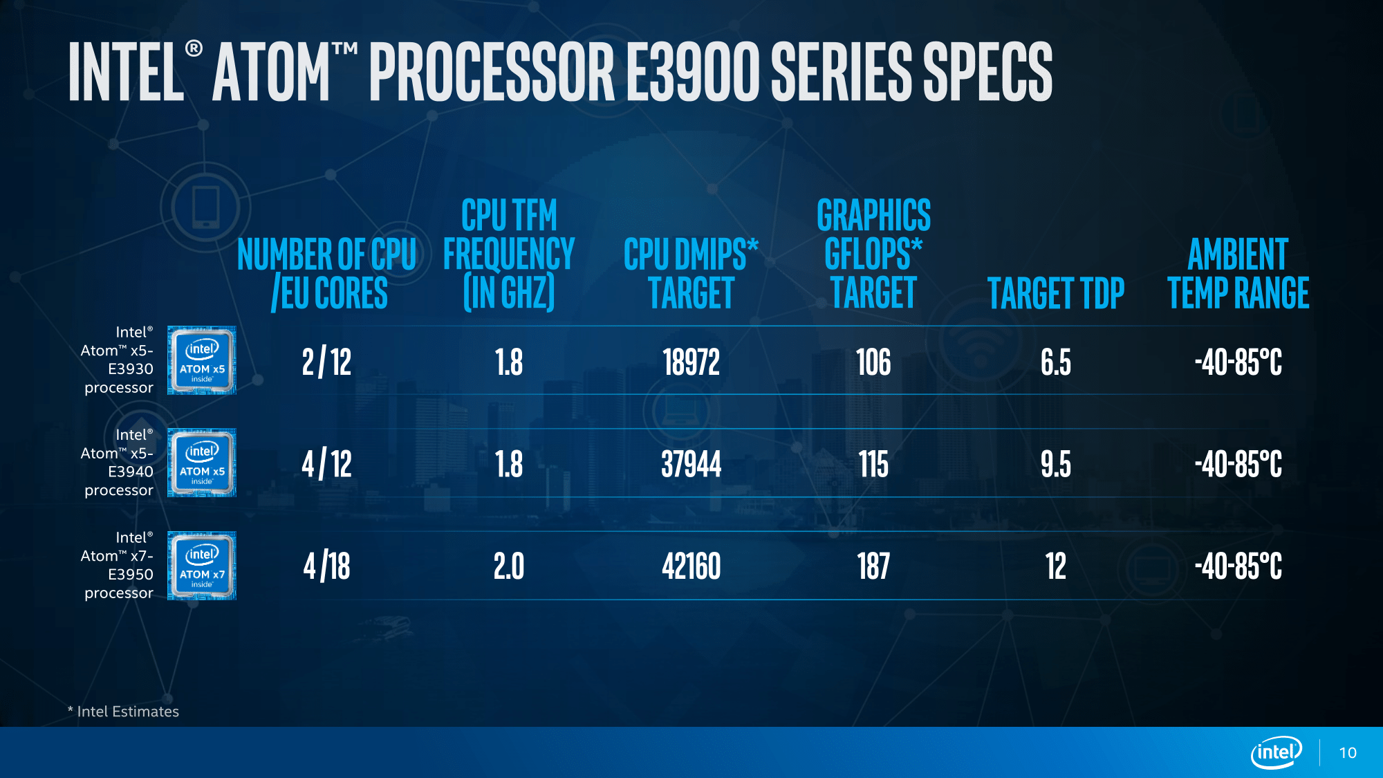
All told, Intel will be offering 3 SKUs of the E3900, ranging from 6.5W to 12W. As relatively high power processors these aren’t meant for wearables and such, but rather primarily devices on mains power where additional intelligence is needed. In Intel terminology, the E3900 is focused on “edge” devices as opposed to “core” devices. The idea being that Intel wants to move out data processing to the edge of an IoT network – into sensors and such devices – as opposed to having to use a dumb sensor that sends data back for processing.
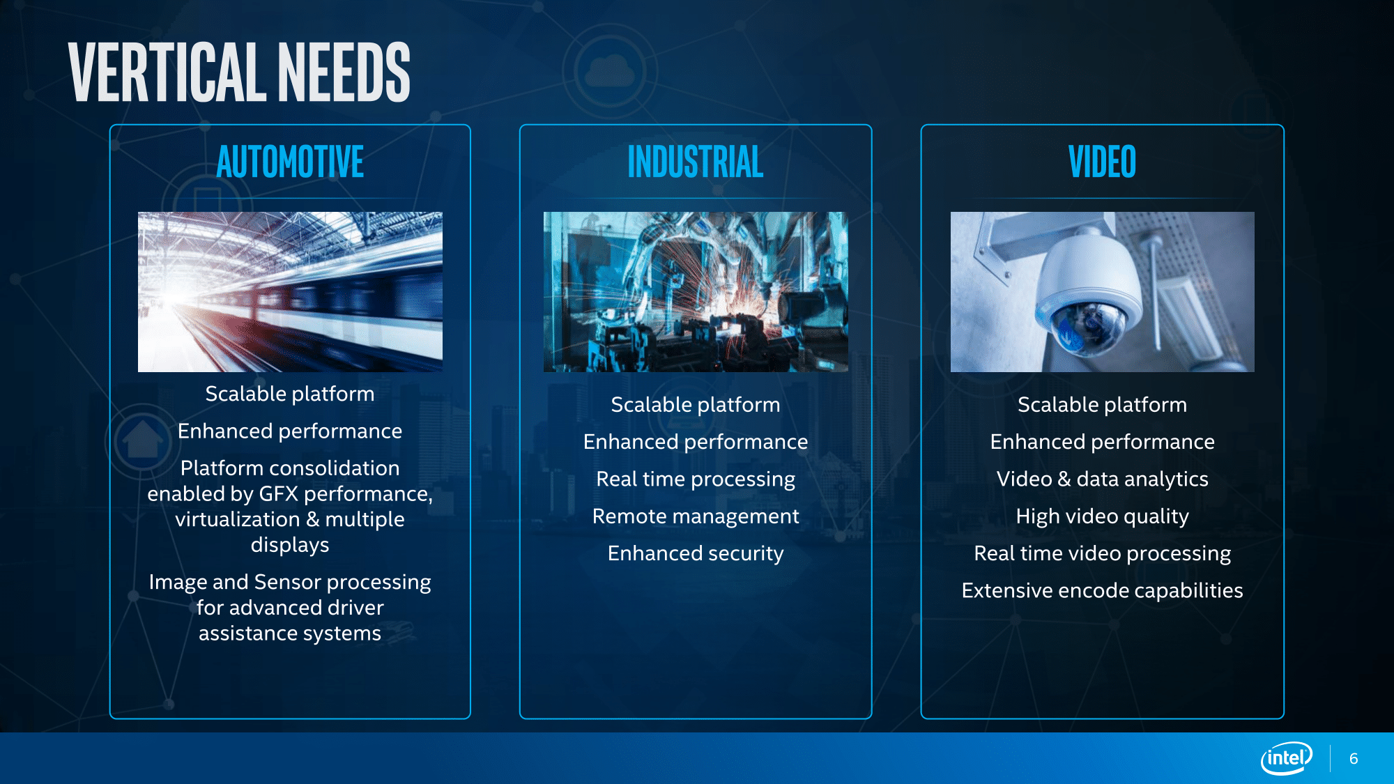
Intel’s 3 big markets here are the video/sensor, industrial, and automotive market. The first and last in particular are areas that the previous E3800 couldn’t readily compete in, due to a lack of processing power for image processing and video encoding. Thanks in big part to the Gen9 GPU and some E3900-specific Image Processing Unit (IPU) changes – the chip can support 15 1080p30 video inputs – Intel can now go after these markets. And that may be the biggest part of this story here for Intel: they haven’t had a part like the E3900 before. The Bay Trail based E3800 had a decent enough CPU, but it’s the E3900 where GPU computing and computer vision become viable, and this is the cornerstone of a lot of new functionality.
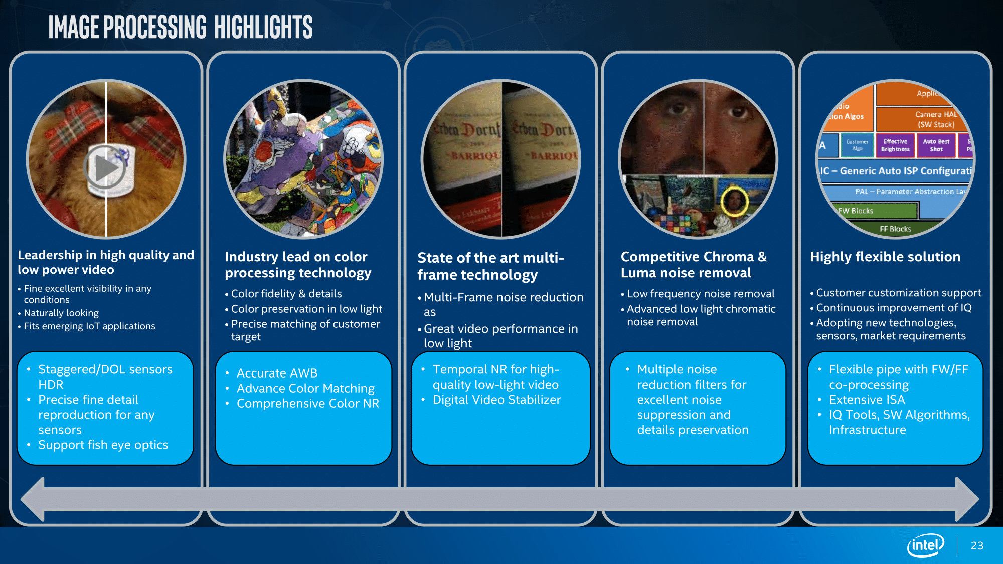
Of course, hardware is only part of the picture. Along with the E3900 itself, Intel will also be shipping a number of software libraries to help developers take better advantage of the hardware, and really, bootstrap the whole process. A good deal of this is on the image processing side, providing functions that tap into the hardware’s new image processing capabilities.
Finally, in the first-half of next year, the E3900 series will be joined by the A3900 series. This is an automotive-specific SKU that is rated for higher operational temperatures; 110C versus 85C for the E3900. As we mentioned before automotive is a big part of Intel’s efforts here, and that means matching automotive tolerances. Given the performance of these chips, we don’t get the impression that Intel’s entering the fully autonomous car market right now, but they are hoping to go after some lower hanging fruit with driver assistance and in-car entertainment systems.


19 Comments
View All Comments
melgross - Tuesday, October 25, 2016 - link
Certainly a major pivot for them. This is much more specialized than previous offerings. It also seems to end the speculation of Intel moving back into the smartphone space.Pork@III - Tuesday, October 25, 2016 - link
106 to 187 GFlops graphic performance may be BADLY low for new generation SoC?BrokenCrayons - Tuesday, October 25, 2016 - link
Agreed. On top of that the TDP target for reaching that level of performance is disappointing as well. Then again, for IoT where the chip is acting as a controller for some sort of black-box device that's constantly fed mains power and doesn't have a the same display responsibilities as a more traditional computing device, it may not matter much.Cygni - Tuesday, October 25, 2016 - link
I don't think you understand what this chip is for.Pork@III - Tuesday, October 25, 2016 - link
If You and Intel maked cut off with "& more" I will be understand...Morawka - Tuesday, October 25, 2016 - link
how much better is Tegra X1 at Graphics performance and at what TDP?SquarePeg - Tuesday, October 25, 2016 - link
Tegra X1 performance as reported here at Anandtech is 512 GFLOPS (FP32) - 1024 GFLOPS (FP16) @ 10 watts.Alexvrb - Tuesday, October 25, 2016 - link
Those X1 performance figures are with the GPU clocked at 1Ghz and a TDP of 15W. The 10W figure is Nvidia's power consumption estimate under who knows what workloads. The only number worth talking about is the 15W TDP.Speaking of which, that's well within the configurable range of Merlin Falcon AMD embedded quadcores. Even at 28nm and configured at a 15W TDP (they can be configured down to 12W), the embedded AMD APUs would be quite competitive with X1. Especially the 8CU models. But Atom and X1 are probably cheaper, and for many embedded applications (such as IoT) you just don't need the oomph. Especially graphics. Fun to talk about though.
hojnikb - Tuesday, October 25, 2016 - link
Will there be any reviews of apollo lake ? I'm very interested in cpu performance and media playback capability.Ryan Smith - Wednesday, October 26, 2016 - link
Yes, there will be. Though I don't have a solid date for you quite yet.