TSMC and Graphcore Prepare for AI Acceleration on 3nm
by Dr. Ian Cutress on August 27, 2020 9:00 AM EST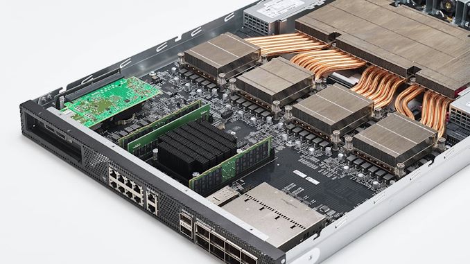
One of the side announcements made during TSMC’s Technology Symposium was that it already has customers on hand with product development progressing for its future 3nm process node technology. As we’ve reported on previously, TSMC is developing its 3nm for risk production next year, and high volume manufacturing in the second half of 2022, so at this time TSMC’s lead partners are already developing their future silicon on the initial versions of the 3nm PDKs.
One company highlighted during TSMC’s presentations was Graphcore. Graphcore is an AI silicon company that makes the IPU, an ‘Intelligence Processing Unit’, to accelerate ‘machine intelligence’. It recently announced its second generation Colossus Mk2 IPU, built on TSMC’s N7 manufacturing process, and featuring 59.2 billion transistors. The Mk2 has an effective core count of 1472 cores, that can run ~9000 threads for 250 Teraflops of FP16 AI training workloads. The company puts four of these chips together in a single 1U to enable 1 Petaflop, along with 450 GB of memory and a custom low-latency fabric design between the IPUs.
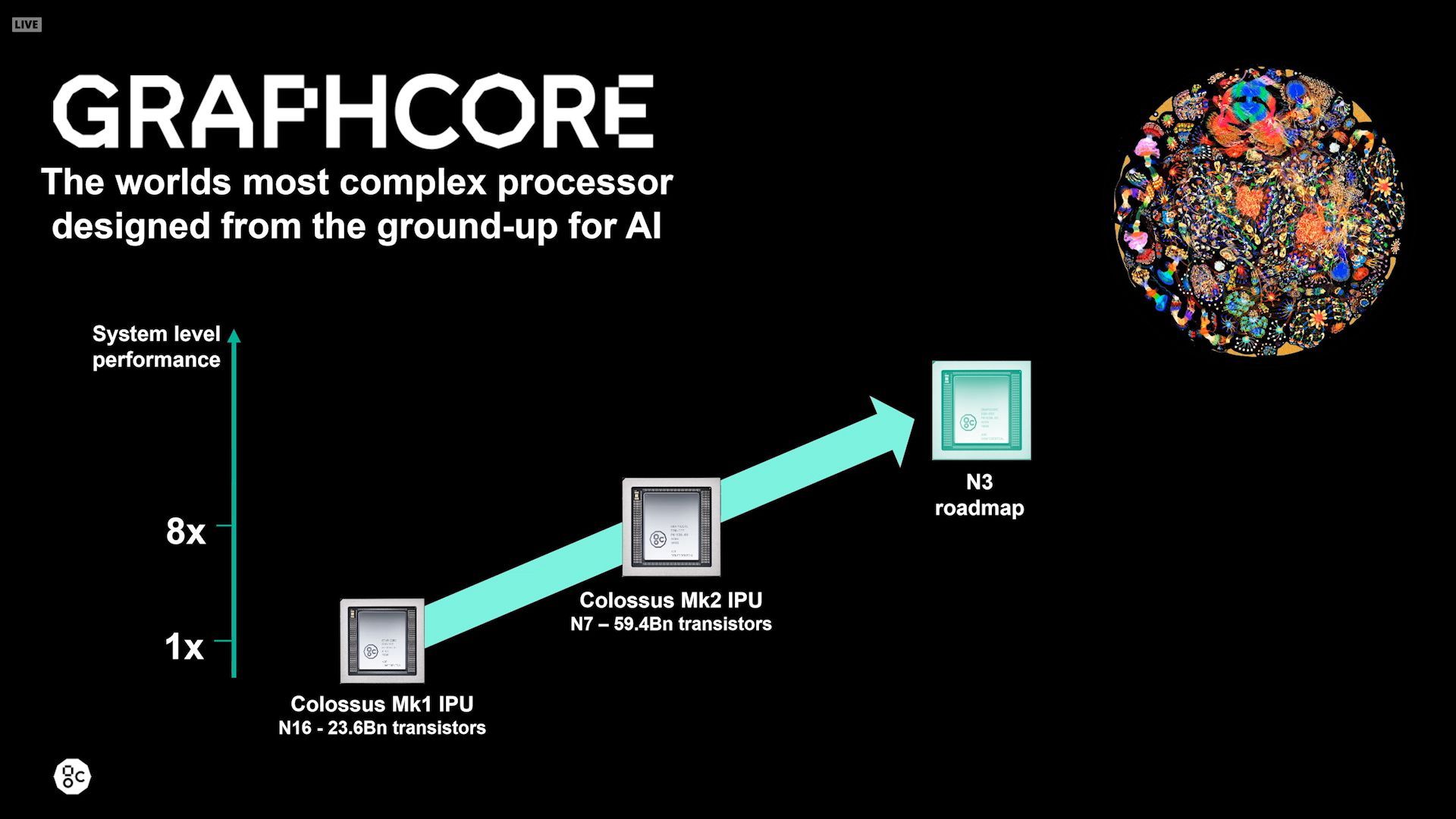
A future generation of products from Graphcore, according to the TSMC presentation, is set to be developed with the TSMC 3nm process in mind, skipping TSMC’s 5nm. No exact timescale was presented, nor any indication of Graphcore’s strategy. As we can see from the slide, the Colossus IPU line involves big high-transistor count chips, using the extra transistor budget afforded by the more dense process node.
We reached out to Graphcore for a statement, and received the following:
Nigel Toon, CEO & co-founder at Graphcore said: “Graphcore was first to build a completely new kind of fully programmable processor, designed from the ground up for machine intelligence. Many of the innovative features of our IPU architecture and the high yields we see even at the cutting edge of the latest process node, are testament to the close technology partnership we enjoy with TSMC. With 59.4Bn transistors, and built using the latest TSMC 7nm technology, the MK2 IPU, which we announced in July, is the world’s most sophisticated processor. Each GC200 IPU has 1472 independent processor cores and an unprecedented 900MB of In-Processor memory delivering an 8x step up in real world performance vs. our MK1 products. We continue to work closely with TSMC as one of their technology innovation partners to explore the advantages of new process nodes and techniques, including N3, so we can continue to deliver more performance improvements to enable our customers to make new breakthroughs in AI.”
PCIe Accelerator with two IPUs

As it stands, Graphcore has a number of products built on its Mk1 and Mk2 IPUs, including systems in partnership with Dell. Graphcore in Q1 2020 went through an extended Series D funding round earlier this year, and has raised $450 million, valuating the company at $1.95 billion, with investors such as BMW, Microsoft, the CEO of DeepMind, and a number of VC firms. According to TechCrunch, who reported this in February, the company still has $300m in cash reserves. As the cost to develop new silicon on the latest manufacturing node increases, it will be interesting to see at what point Graphcore puts an order in with TSMC’s 3nm, or if TSMC and Graphcore are working together to help optimize the process for large scale chips and if TSMC will bear some of that cost.
Related Reading
- TSMC Details 3nm Process Technology: Full Node Scaling for 2H22 Volume Production
- TSMC To Build 5nm Fab In Arizona, Set To Come Online In 2024
- TSMC & Broadcom Develop 1,700 mm2 CoWoS Interposer: 2X Larger Than Reticles
- TSMC Boosts CapEx by $1 Billion, Expects N5 Node to Be Major Success
- Early TSMC 5nm Test Chip Yields 80%, HVM Coming in H1 2020
- TSMC: 5nm on Track for Q2 2020 HVM, Will Ramp Faster Than 7nm
- TSMC: N7+ EUV Process Technology in High Volume, 6nm (N6) Coming Soon


1 Comments
View All Comments
Gondalf - Wednesday, September 2, 2020 - link
Better 5nm work well, look like idiotic to speak about 3nm right now.TSMC clearly fear a lot Samsung competition, Samsung have all the resources to be 50% of Foundry market very shortly.
It is unconfortable to face a so big and rich company like Samsung.