ARM Announces Mali 800 Series GPUs - T860, T830, & T820
by Ryan Smith on October 27, 2014 10:31 PM EST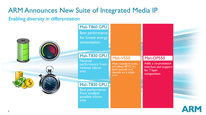
Due to a lack of total vertical integration and heavy focus on IP licensing, one of the more interesting aspects of the SoC development pipeline is that we get to see the architectures and chips developed and announced in a very decoupled fashion. As opposed to the PC industry where there is heavy vertical integration and architectures are usually announced close to (if not at the same time as) the first silicon and even the first finished products, in the SoC space we will frequently see the complete development cadence in public – architectures, chips, and finally finished products. This has its own ups and downs, and while it means we’ll potentially hear about a new architecture long before it’s available in a product, on the other hand we get a lot more visibility into what’s coming down the development pipeline, at least for companies that develop IP for licensing or purchase it for use in their SoCs.
This brings us to the matter of ARM and today’s announcements. As a massive ISA, CPU, and GPU licenser, ARM’s product lineup is the textbook case for early visibility. At a time when the first high-end 20nm SoCs are just now hitting consumer devices in products such as the Samsung Galaxy Note 4 International and Apple iPhone 6, ARM’s development pipeline and product marketing teams are already looking at next year’s products and what processor designs to prepare for them. For ARM’s GPU group in particular, whom now functionally operates on a yearly release cadence, the roll-out of Mali 700 equipped devices means that it’s time to announce the designs for next year’s GPUs.
To that end, today ARM is announcing the Mali 800 series. Designed for inclusion in 2015+ SoCs, the Mali 800 series is the immediate successor to the current Mali 700 series. From an architectural standpoint Mali 800 is still based on the same common Midgard architecture that the Mali 600 and Mali 700 series are based on, and as a result from an architectural standpoint there isn’t much to discuss. Midgard and its unusual all-ILP/no-TLP architecture is still a modern GPU architecture that supports up to OpenGL ES 3.1, the Android Extension Pack, and Direct3D 11.1, so from that standpoint ARM has little reason to change.
Consequently while still based on Midgard, the 800 series is a successive round of optimization for the Midgard designs. For this generation ARM has focused on further improving Midgard’s area and power efficiency while adding a handful of new features not found in the existing Mali 700 series. This refresh spans from ARM’s highest-end designs to lowest-end designs, and coupled with Mali’s multi-core scalability spans the SoC GPU market from top to bottom.
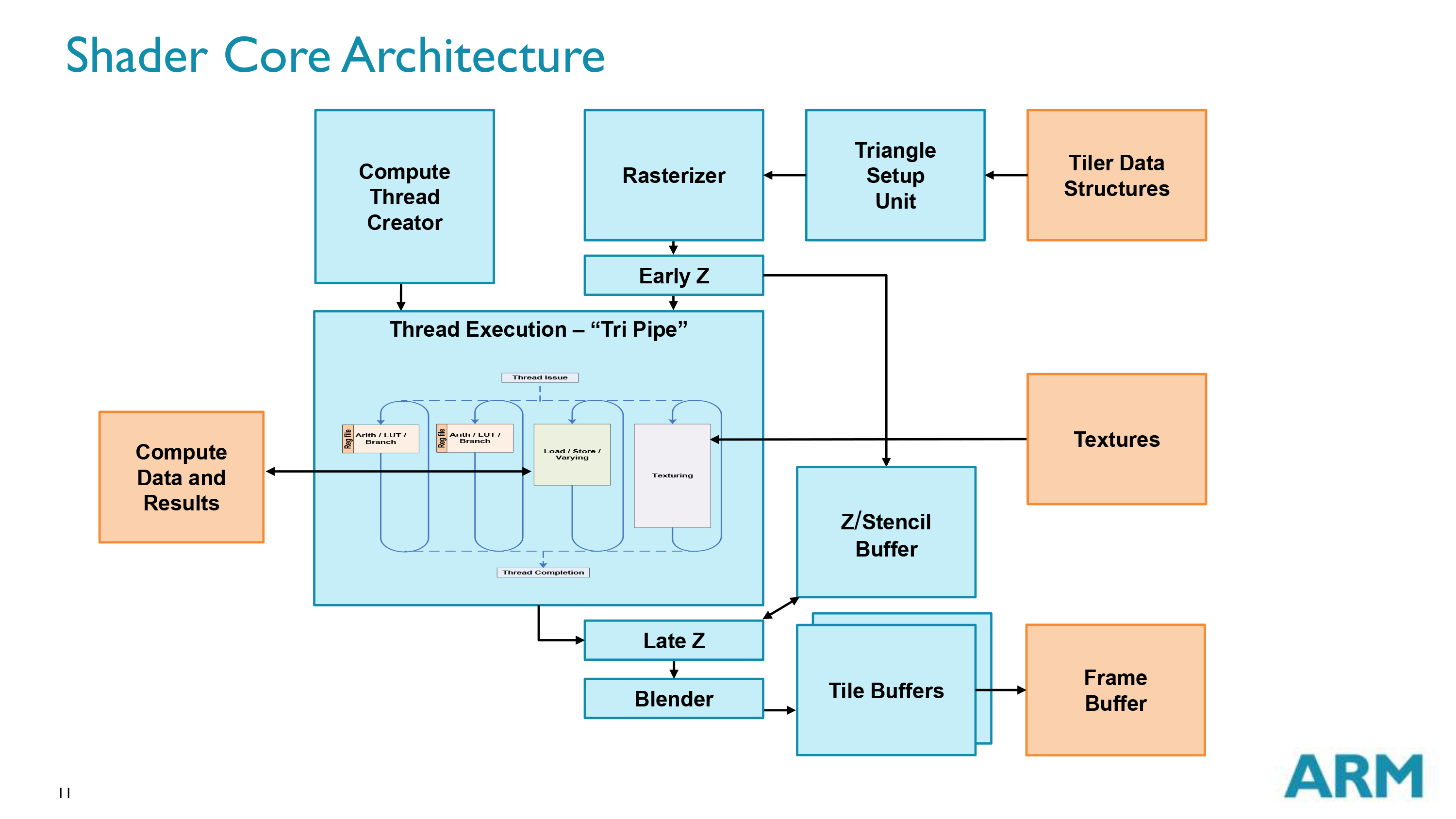
The Midgard Shader Core
| ARM Mali 800 Series | |||||
| T860 | T830 | T820 | |||
| Core Configurations | 1-16 | 1-4 | 1-4 | ||
| ALU Pipes Per Core | 2 | 2 | 1 | ||
| Texture Units Per Core | 1 | 1 | 1 | ||
| FLOPs (FP32 MAD) | 20 - 320 FLOPs | 20 - 80 FLOPs | 10 - 40 FLOPs | ||
| OpenGL ES | ES 3.1 + AEP | ES 3.1 + AEP | ES 3.1 + AEP | ||
| Direct3D | FL 11_1 | FL 9_3 | FL 9_3 | ||
| 10-Bit YUV | Yes | Optional | Optional | ||
Mali-T860
We’ll start off with ARM’s new high-end Mali design, the Mali-T860. With ARM reforming their product naming with the Mali 700 series ARM’s lineup is now much easier to follow, and as given away by the T860’s design it’s the immediate successor to the T760.
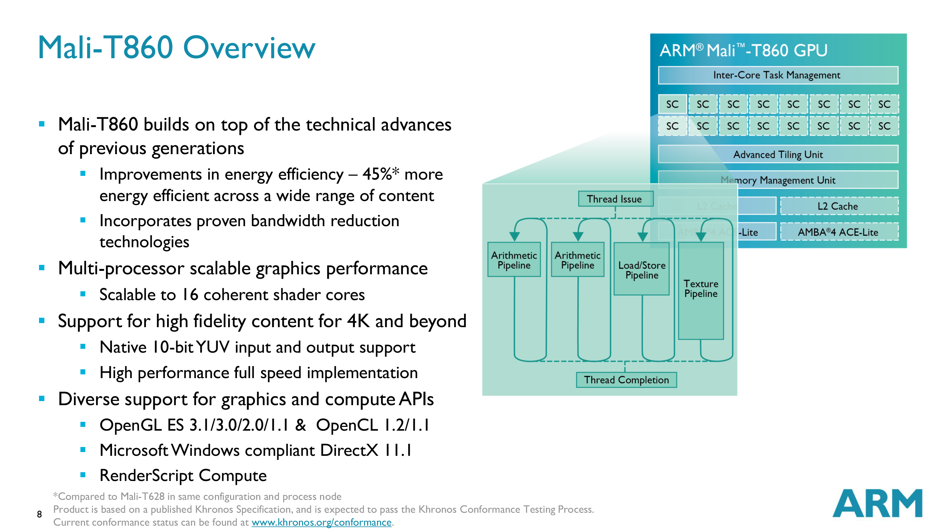
Like T760 before it, T860 is ARM’s most feature packed and most powerful Mali design. The underlying design uses the more common Midgard 2 arithmetic pipelines per core configuration, with the overall design being scalable to up to 16 cores. Coupled with the single texture unit per core, the throughput of a T860 design can scale from 20 FLOPs (10 MADs) and 1 texel per clock up to 320 FLOPs and 16 texels per clock. As a result this design can also be scaled up and down as needed to cover both phones and tablets just by varying the number of cores.
From a functionality standpoint, T860 will be the only Mali 800 part to support the 800 series’ fullest feature set. Specifically, support for Direct3D feature level 11_1 is limited to T860. Otherwise common to the entire 800 series, T860 also supports OpenGL ES 3.1, the Android Extension Pack, and OpenCL 1.2.
Meanwhile one notable feature addition for the Mali 800 family is support for native (and full speed) 10-bit YUV input and output. At the moment this feature addition is going to be of limited value, but HEVC is expected to make significant use of 10-bit YUV, so adding support here is laying the groundwork for HEVC in future products, and for that matter will go hand-in-hand with ARM’s new video processing block and display controller block, which are also being announced today.
Elsewhere from a performance standpoint ARM is offering the usual high level performance estimates. However it should be noted that these are compared to the two-generation old T628, and there aren’t similar numbers to work from for T760. In any case, compared to T628 ARM expects an equal configuration T860 to be some 45% more energy efficient on the same process node. And seeing as how mobile performance gains are almost entirely an exercise in energy efficiency, this would represent a very significant increase in energy efficiency (and ultimately sustainable performance) for their designs.

ARM Frame Buffer Compression - From Our Look at Midgard Earlier This Year
That said, by making a two-generation old comparison ARM also gets to roll up the benefits of their AFBC frame buffer compression technology, which was first introduced on the Mali 700 series. AFBC is something the company is significantly banking on due to the high bandwidth savings, and ARM considers one of their greatest feature advantages for the 800 series as well as the 700 series.
Finally, something to also keep in mind though is that while ARM’s same-node comparison is the fairest way to look at architectural efficiency, you’re highly unlikely to see T628 manufactured on 20nm+ processes. So on top of the architectural gains over the years, the real world performance gains for T860 should be better still due to the newer process node.
Mali-T830 & Mali-T820
Also being announced today alongside the T860 and rounding out the new Mali 800 family are the T830 and T820. These parts are best described as ARM’s low-end and mainstream designs, and are the successors to the T720. With Mali T860 essentially scaling down to cover most of the mid-range, the T820 and T830 are intended to be lower performance, lower power consuming parts that are optimized around power and die size needs.
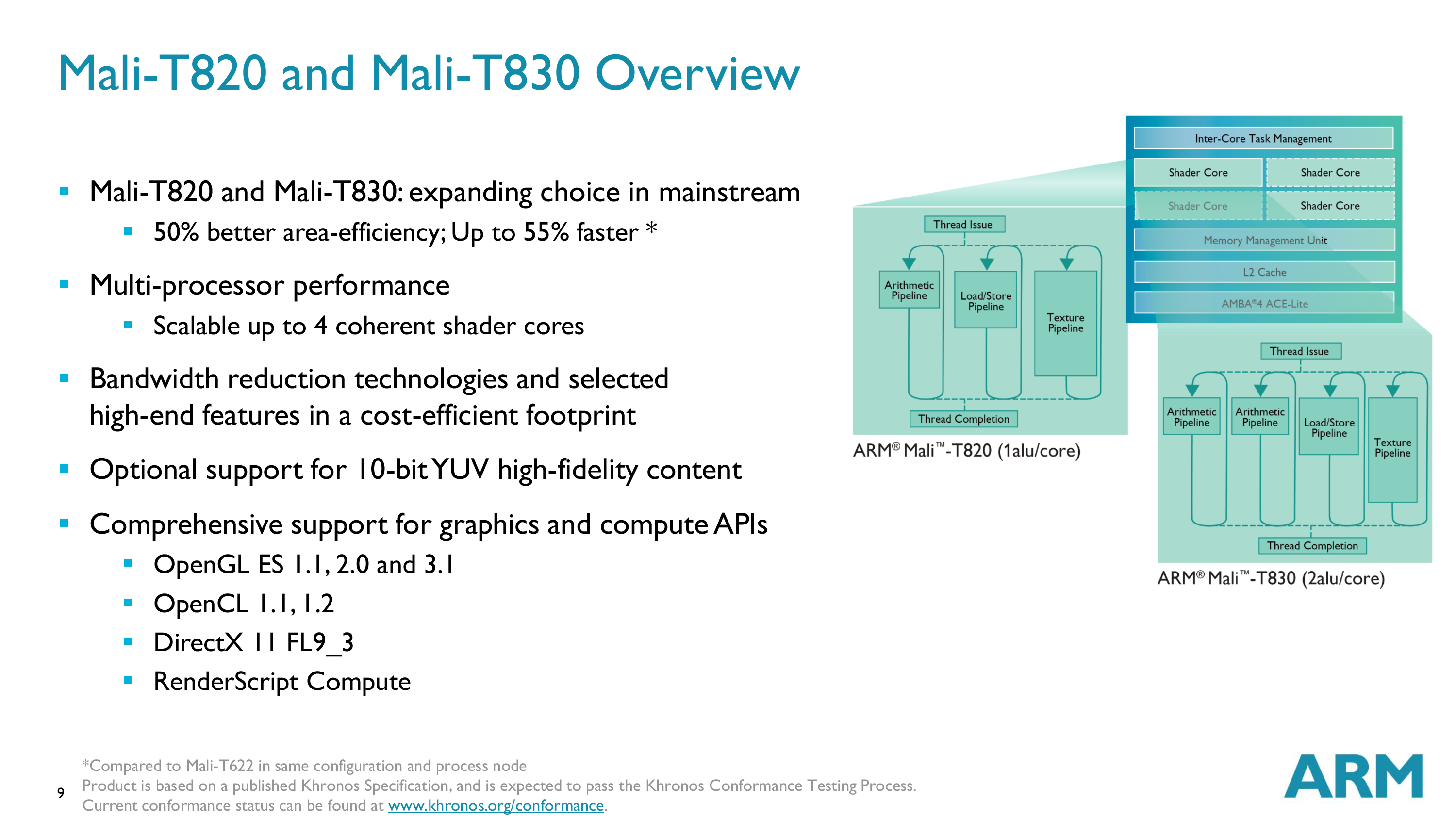
For the Mali 800 series ARM is bifurcating the T720’s market a bit to offer different blends of die size and performance. The T720’s immediate successor is the T820, and like its predecessor is a one arithmetic pipeline design that is focused first and foremost on die size. Meanwhile new to the 800 series, though still a successor of sorts to the T720, is the Mali-T830. This is a more powerful design that while still focused on die size efficiency brings the number of pipelines to two per core (like T860), offering better performance in exchange for a slightly larger die size.
Other than the difference in the number of pipelines, the T820 and T830 designs are extremely similar. Both of them can be scaled up to 4 cores, allowing for some performance scaling. This puts the throughput of T820 designs at a range of 10 FLOPs and 1 texel per clock to 40 FLOPs and 4 texels per clock, while T830 will scale from 20/1 to 80/4 respectively.
From a feature standpoint, as previously mentioned only T860 gets the fullest Mali feature set while the other Mali 800 parts will be a bit more modest. T830 and T820 only support Direct3D up to feature level 9_3, while for the more mobile-centric world they will be on par with the T860 and support OpenGL ES 3.1 and the Android Extension Pack. Meanwhile 10-bit YUV support is present here, however for T820 and T830 it is an optional feature that will depend on which specific version of the core is licensed, so we will likely see a mix of retail products that do and do not include it.
Finally from a performance standpoint ARM is once again offering some high level guidance compared to the Mali 600 series, specifically the Mali-T622 in this case. Depending on the 800 design used, ARM tells us that performance should be up to 55% better or area efficiency will be 50% better. Presumably the area efficiency comparison is for T820 while the performance comparison is for T830.
Closing Thoughts
Launching alongside the new Mali GPUs today are a series of updates for the rest of ARM’s graphics stack, which will see the Mali-V video block and Mali-DP display controllers updated respectively. Along with the general strength of the Mali GPUs, expect to see ARM focus heavy on the synergy between these parts, including their common support for AFBC and of course the benefits of having all graphics components developed together. We’re covering these in another article, but we wanted to quickly point out where the Mali GPUs fit in the bigger picture of ARM’s announcements today.

Finally, while ARM doesn't have complete control over consumer devices (since they only sell designs to chipmakers) they are providing a rough estimate of when to expect Mali 800 GPUs to begin appearing in devices. According to ARM we should expect to start seeing Mali 800 devices starting in late 2015, or roughly a year from now. This is consistent with the Mali 700 series, which having been announced almost a year ago to this day has started to show up in consumer devices very recently. To that end we would expect to start seeing Mali 800 SoC designs announced in the first half of next year, with consumer designs to follow as per ARM's timetable.


28 Comments
View All Comments
darkich - Tuesday, October 28, 2014 - link
Well this was unexpected.The Artemis and Maya(likely successors to the A53/57) CPU cores are still yet to be announced despite of ARM clearly hinting about them for months now.
przemo_li - Tuesday, October 28, 2014 - link
Not really.GPU division was split from CPUs some time ago. Now those are two separate entities. They pursue different schedules and different strategies.
darkich - Tuesday, October 28, 2014 - link
Maybe Artemis and Maya are actually the two video processors also announced today?I hope that's not true though.
It is ime for the new CPU announcement as well. The A5x have reached the market, and unless ARM significantly speeds up the product cycles, it could find itself behind the curve ( Krait successor should be out next year, and Cyclone and Denver are already very competitive, with their superior single threaded performance)
michael2k - Tuesday, October 28, 2014 - link
Wait, when did we ever expect them to be ahead of the curve? The only reason the curve looks different is that Apple's A7 came out last year ahead of anyone's expected timetable. Had it been released this year (as the industry expected) it would have come out alongside the A53/A57 parts and the Tegra K1 Denver part, and only a couple quarters ahead of Krait.ARM doesn't need to be ahead of the curve, per se, it only needs to be competitive, and until the Denver moves down to smartphones and the Krait comes out, there is no part more suitable for smartphones than the A5X cores.
darkich - Wednesday, October 29, 2014 - link
Well that's the thing, judging by previous record it takes at least two years for newly announced ARM CPU to reach the market.And the successor to Krait should show up in phones much sooner than that, supposedly in about one year.
michael2k - Wednesday, October 29, 2014 - link
Right, but that's only because Apple upset the cart. Had the A7 been released this year the Krait would have hustled and been out in 2017, and everything would be as expected. However, Apple released the A7 in 2013, everyone said, "OH NO", the Denver got out this year (hotter than expected) and the Krait in 2015 instead.Tigran - Tuesday, October 28, 2014 - link
And what does "scalable to up to 16 [shader] cores"? Isn't there a definite number (which one?) of shader cores in Mali-T860?spellegrini - Tuesday, October 28, 2014 - link
The design supports up to 16 cores. Said that, who implements the design (e.g. Samsung LSI) will decide how many cores to configure the GPU with.Tigran - Tuesday, October 28, 2014 - link
Thank you. And how can I know number of shader cores in some particular SoC, is there any abbreviation in it's name?Ryan Smith - Tuesday, October 28, 2014 - link
Yes. The typical nomenclature is [GPU model]MP[number of cores. e.g. Mali-T860MP8