3nm
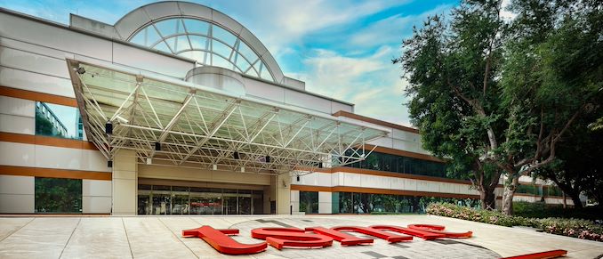
Taiwan Semiconductor Manufacturing Co. this week said its revenue for the second quarter 2024 reached $20.82 billion, making it the company's best quarter (at least in dollars) to date. TSMC's high-performance computing (HPC) platform revenue share exceeded 52% for the first time in many years due to demand for AI processors and rebound of the PC market. TSMC earned $20.82 billion USD in revenue for the second quarter of 2024, a 32.8% year-over-year increase and a 10.3% increase from the previous quarter. Perhaps more remarkable, $20.82 billion is a higher result than the company posted Q3 2022 ($20.23 billion), the foundry's best quarter to date. Otherwise, in terms of profitability, TSMC booked $7.59 billion in net income for the quarter, for a gross margin of...
Samsung Foundry Vows to Surpass TSMC Within Five Years
The head of Samsung's semiconductor unit acknowledged last week that the company's current mass production, leading-edge process technologies are a couple of years behind TSMC's most advanced production nodes...
18 by Anton Shilov on 5/8/2023
TSMC Announces Early Access Nodes for Next-Gen Car Chips: N4AE and N3AE
As the final set of announcements from this week's North American Technology Symposium, TSMC closed out their fab roadmap updates with some fresh news on their automotive-centric processes. For...
10 by Anton Shilov on 4/28/2023
TSMC Details 3nm Evolution: N3E On Schedule, N3P and N3X To Deliver 5% Performance Gains
Alongside some new announcements for their 2nm process node plans, TSMC has also released a progress and roadmap update for their N3 family process technologies at today's 2023 North...
13 by Anton Shilov on 4/26/2023
Synopsys Intros AI-Powered EDA Suite to Accelerate Chip Design and Cut Costs
Synopsys has introduced the industry's first full-stack AI-powered suite of electronic design automation tools that covers all stages of chip design, from architecture to design and implementation to manufacturing...
12 by Anton Shilov on 3/30/2023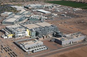
Inflation Drives Up Fab Costs for Intel and Samsung by Billions of Dollars
To address future demand for semiconductors amid severe chip shortages of 2020 – 2022, all leading chipmakers announced plans to build new fabs and even disclosed their estimated costs...
15 by Anton Shilov on 3/16/2023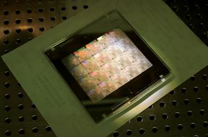
TSMC's 3nm Journey: Slow Ramp, Huge Investments, Big Future
Last week, TSMC issued their Q4 and full-year 2022 earnings reports for the company. Besides confirming that TSMC was closing out a very busy, very profitable year for the...
30 by Anton Shilov on 1/17/2023
TSMC Unveils Major U.S. Fab Expansion Plans: 3nm and $40 Billion by 2026
TSMC this week held its Arizona fab 'first tool-in' ceremony, where alongside celebrating its first US fab, the company also announced major expansion plans for the production facility. The...
17 by Anton Shilov on 12/7/2022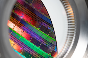
TSMC and ASML: Demand for Chips Remains Strong, But Getting Fab Tools Is Hard
TSMC's revenue this year is going to set an all-time record for the company, thanks to high demand for chips as well as increased prices that its customers are...
13 by Anton Shilov on 7/21/2022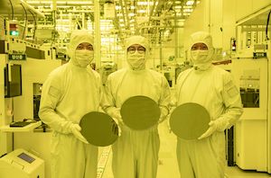
Samsung Starts 3nm Production: The Gate-All-Around (GAAFET) Era Begins
Capping off a multi-year development process, Samsung’s foundry group sends word this morning that the company has officially kicked off production on its initial 3nm chip production line. Samsung’s...
22 by Ryan Smith on 6/30/2022
TSMC Readies Five 3nm Process Technologies, Adds FinFlex For Design Flexibility
Taiwan Semiconductor Manufacturing Co. on Thursday kicked off its 2022 TSMC Technology Symposium, where the company traditionally shares it process technology roadmaps as well as its future expansion plans...
44 by Anton Shilov on 6/16/2022
Applied Materials Outlines Next-Gen Tools for 3nm and GAA Transistor Era
Last month Samsung Foundry quietly announced that it was set to begin producing chips using its 3GAE (3 nm-class, gate-all-around transistors, early) process technology in the second quarter. While...
17 by Anton Shilov on 5/12/2022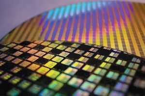
TSMC Roadmap Update: N3E in 2024, N2 in 2026, Major Changes Incoming
Taiwan Semiconductor Manufacturing Co. has solid plans for the next few years, but the foundry's manufacturing technology design cycles are getting longer. As a result, to address all of...
21 by Anton Shilov on 4/22/2022
TSMC Roadmap Update: 3nm in Q1 2023, 3nm Enhanced in 2024, 2nm in 2025
TSMC has introduced a brand-new manufacturing technology roughly every two years over the past decade. Yet as the complexity of developing new fabrication processes is compounding, it is getting...
32 by Anton Shilov on 10/18/2021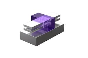
Samsung Foundry: 2nm Silicon in 2025
One of the key semiconductor technologies beyond 3D FinFET transistors are Gate-All-Around transistors, which show promise to help extend the ability to drive processors and components to higher performance...
29 by Dr. Ian Cutress on 10/6/2021
Samsung: Deployment of 3nm GAE Node on Track for 2022
Samsung Foundry has made some changes to its plans concerning its 3 nm-class process technologies that use gate-all-around (GAA) transistors, or what Samsung calls its multi-bridge channel field-effect transistors...
32 by Anton Shilov on 7/9/2021
An AnandTech Interview with TSMC: Dr. Kevin Zhang and Dr. Maria Marced
In the past week, TSMC ran its 2021 Technology Symposium, covering its latest developments in process node technology designed to improve the performance, costs, and capabilities for its customers...
18 by Dr. Ian Cutress on 6/8/2021
TSMC Update: 2nm in Development, 3nm and 4nm on Track for 2022
For TSMC, being the world's largest foundry with nearly 500 customers has its peculiarities. On the one hand, the company can serve almost any client with almost any requirements...
74 by Anton Shilov on 4/26/2021
TSMC to Spend $100B on Fabs and R&D Over Next Three Years: 2nm, Arizona Fab & More
TSMC this week has announced plans to spend $100 billion on new production facilities as well as R&D over the next three years. The world's largest contract maker of...
45 by Anton Shilov on 4/2/2021
Samsung Foundry: New $17 Billion Fab in the USA by Late 2023
Samsung Foundry has filed documents with authorities in Arizona, New York, and Texas seeking to build a leading-edge semiconductor manufacturing facility in the USA. The potential fab near Austin...
36 by Anton Shilov on 2/10/2021
TSMC and Graphcore Prepare for AI Acceleration on 3nm
One of the side announcements made during TSMC’s Technology Symposium was that it already has customers on hand with product development progressing for its future 3nm process node technology...
2 by Dr. Ian Cutress on 8/27/2020


